A Clock Generating Circuit for Analog-to-Digital Converter

A clock generation circuit, analog-to-digital converter technology, applied in the direction of generating electrical pulses, pulse generation, electrical components, etc., can solve the problems of deteriorating ADC signal-to-noise ratio, wrong sampling of analog input signal amplitude, wrong trigger sampling time, etc., to achieve Improve the ADC signal-to-noise ratio, reduce harsh requirements, and improve the effect of clock signal quality

Active Publication Date: 2019-09-17
TIANJIN UNIV
View PDF6 Cites 0 Cited by
  • Summary
  • Abstract
  • Description
  • Claims
  • Application Information

AI Technical Summary

Problems solved by technology

The jitter generated by the clock signal will cause the internal circuit of the ADC to incorrectly trigger the sampling time, resulting in missampling of the analog input signal in amplitude, thereby deteriorating the signal-to-noise ratio of the ADC

Method used


Image

  • A Clock Generating Circuit for Analog-to-Digital Converter
  • A Clock Generating Circuit for Analog-to-Digital Converter
  • A Clock Generating Circuit for Analog-to-Digital Converter

Examples


Embodiment Construction

[0019] The present invention will be further described in detail below in conjunction with specific embodiments.

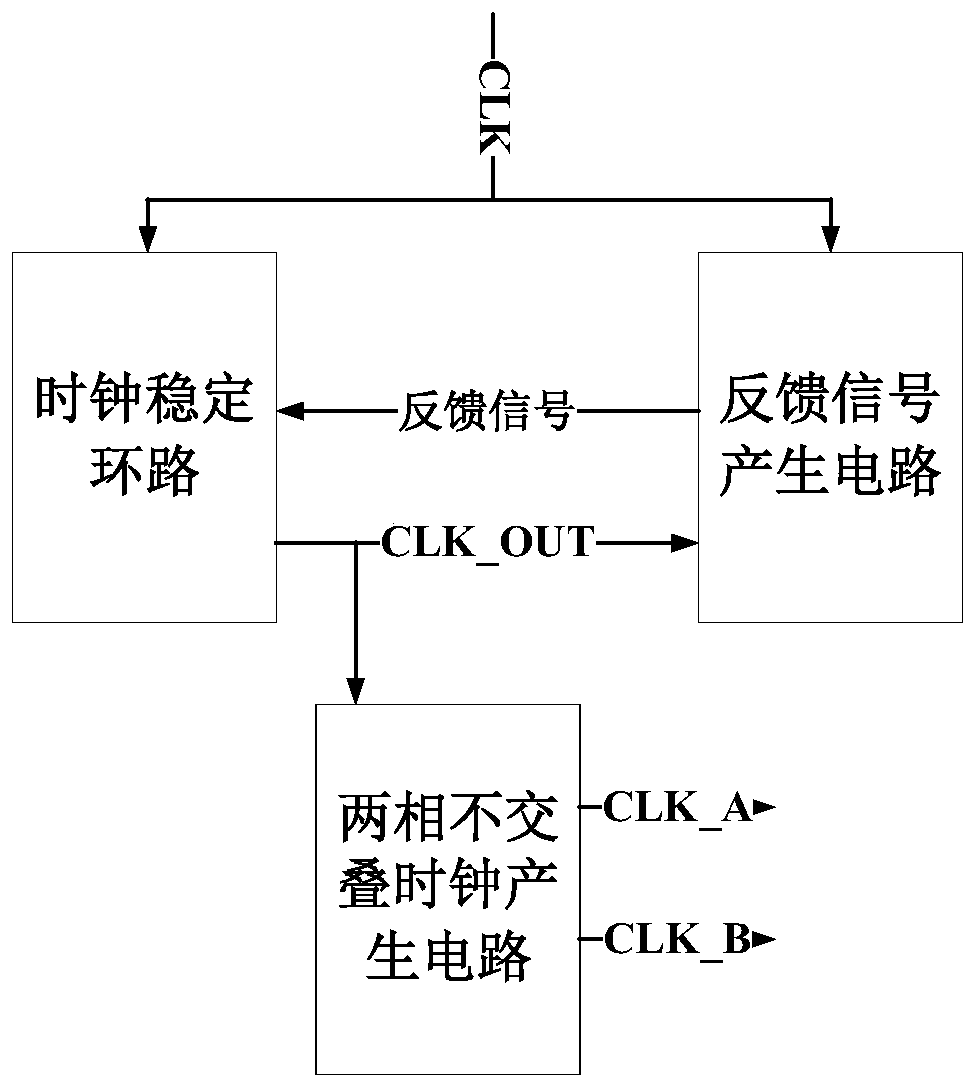
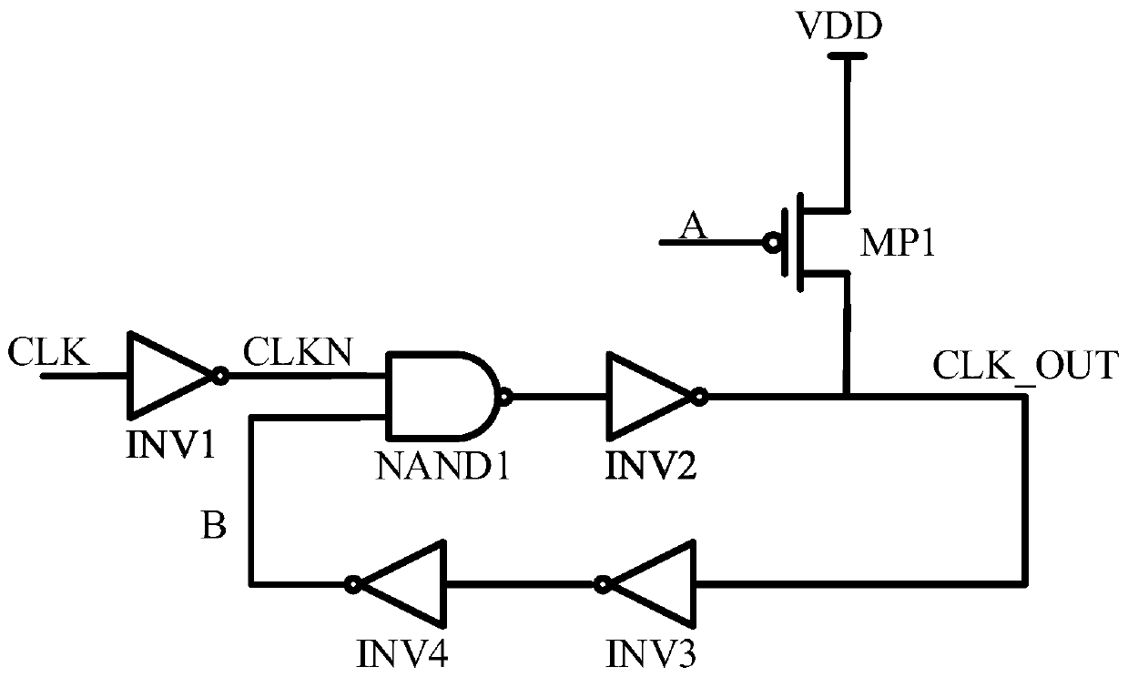
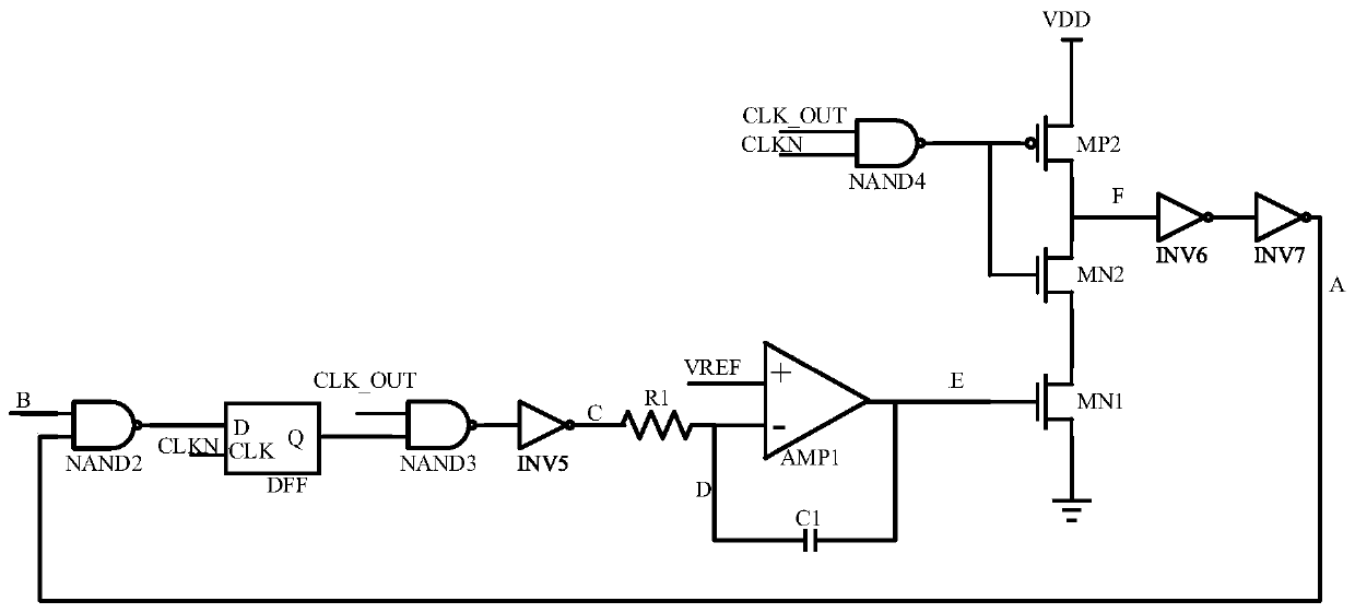
[0020] Such as figure 1 As shown, the design idea of ​​the present invention is to generate a stable clock signal through a clock stabilization loop, and the used clock stabilization loop itself can reduce the duty cycle of the output clock signal CLK_OUT through the NAND gate NAND1, and increase the duty cycle by pulling up the PMOS tube MP1 Output clock signal CLK_OUT duty cycle. Through the feedback signal generating circuit part, the feedback signal A is generated according to the input clock CLK and the output clock CLK_OUT, so as to realize the duty cycle adjustment of the output clock and the elimination of clock jitter.

[0021] Such as figure 1 As shown, a clock generation circuit for an analog-to-digital converter proposed by the present invention includes a clock stabilization circuit and a two-phase non-overlapping clock generation circuit. The clock stabil...


PUM


Abstract

The invention discloses a clock generation circuit for an analog-to-digital circuit, which comprises a clock stabilizing circuit and a two-phase non-overlapping clock generation circuit. The clock stabilizing circuit comprises a clock stabilizing loop and a feedback signal generation circuit. In the feedback signal generation circuit, a control signal is generated by an active low-pass filter to control an N tube current modulation inverter, the clock stabilizing loop is used for generating a stable clock signal, and by a filtering technology and a current modulation technology, accurate modulation on a feedback signal is implemented. In the clock stabilizing loop, by a loop structure, a duty ratio of an output clock can be reduced; under the regulation of the feedback signal, by pulling up a PMOS tube MP1, the duty ratio of the output clock is increased, and finally, the duty ratio of 50% of the output clock is achieved; and the clock is stabilized and vibration is reduced. According to the clock generation circuit disclosed by the invention, the clock stabilizing circuit can be integrated into an ADC circuit; and by adopting the structure disclosed by the invention, clock signal quality can be obviously improved, the strict requirement of an ADC for clock quality is reduced, and a signal-to-noise ratio of the ADC is improved.

Description

Technical field [0001] The invention relates to the field of analog integrated circuits, and in particular to a clock generation circuit structure that can be used in a digital analog mixed signal circuit. Background technique [0002] In the process of human beings exploring nature by using technology and wisdom, the first signal obtained is an analog signal, and computers can only process digital signals. It is necessary to quantify the widely existing analog signals in nature into digital signals through an analog-to-digital converter to facilitate people to use computers for processing and transmission. Therefore, the analog-to-digital converter is a bridge between the analog world and the digital world, and has important use value and broad application prospects. [0003] With the continuous development of ADCs (analog-to-digital converters) towards high-speed and high-precision, the error caused by the phase noise caused by the sampling clock jitter on the sample-and-hold ci...

Claims


Application Information

Patent Timeline
Patent Type & Authority Patents(China)
IPC IPC(8): H03M1/08H03K3/017
Inventor 赵毅强王佩瑶赵公元辛睿山胡凯高曼
Owner TIANJIN UNIV
Why Eureka
Try Eureka