A clock multiplier circuit

A clock frequency multiplication and circuit technology, applied in the field of electronics, can solve the problems of design modification limitation, high design cost, large resource occupation, etc., and achieve the effect of avoiding frequency range requirements, low design cost, and small resource occupation.

Active Publication Date: 2018-04-13
NATIONZ TECH INC
View PDF8 Cites 0 Cited by
  • Summary
  • Abstract
  • Description
  • Claims
  • Application Information

AI Technical Summary

Problems solved by technology

The disadvantage is that the phase-locked loop has a certain bandwidth and has requirements on the frequency range of the input clock, so it can only perform frequency multiplication processing on clocks in a certain frequency range. For example, the devices with phase-locked loops produced by some logic device manufacturers only It can perform frequency multiplication processing on a clock not higher than 25MHz, so this design method limits the design modification. In addition, if the phase-locked loop technology is implemented in a logic device without a phase-locked loop, the resource occupation is large and the design cost is high. , if the phase-locked loop technology is implemented through circuit design, it will increase the complexity of the circuit and the difficulty of debugging, and the design cost will be higher
[0006] Therefore, existing implementations are not perfect enough

Method used


Image

  • A clock multiplier circuit
  • A clock multiplier circuit
  • A clock multiplier circuit

Examples


Embodiment Construction

[0029] The present invention will be further described in detail below through specific embodiments in conjunction with the accompanying drawings.

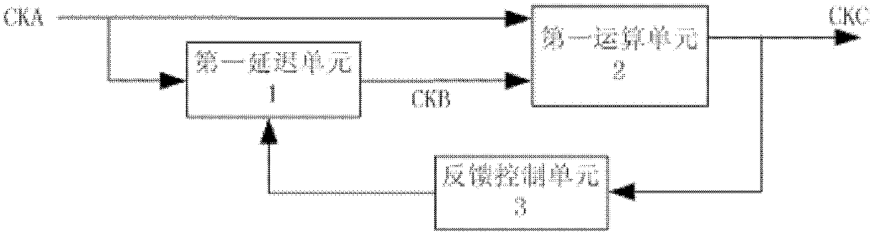
[0030] Such as figure 1 As shown, a clock multiplication circuit according to an embodiment of the present invention includes a first delay unit 1 , a first operation unit 2 and a feedback control unit 3 .

[0031] Wherein, one input terminal of the first delay unit 1 is connected to an externally input clock signal CKA, the other input terminal is connected to the control signal input by the feedback control unit 3, and the output terminal is connected to an input terminal of the first computing unit 2, and the feedback control unit 3 The input control signal is used as a delay parameter for delay processing by the first delay unit 1, and the first delay unit 1 delays the externally input clock signal CKA according to the delay parameter to obtain a clock delay clock signal CKB, and outputs CKB to the first Arithmetic Unit 2.

...


PUM


Abstract

The invention discloses a clock frequency multiplication circuit. The clock frequency multiplication circuit includes a first delay unit, a first operation unit and a feedback control unit, wherein, under the control of the feedback control unit, the first delay unit converts the externally input clock The signal is delayed and processed to obtain and output a delayed clock signal; the first computing unit performs logic operations according to the clock signal input from the outside and the delayed clock signal output by the first delay unit to obtain and output a multiplied clock signal; the feedback control unit according to The multiplied clock signal output by the first operation unit controls the delay processing of the first delay unit. Through the above technical solutions, the present invention provides a more complete clock frequency multiplication circuit.

Description

technical field [0001] The invention relates to the field of electronics, in particular to a clock frequency multiplication circuit. Background technique [0002] The clock multiplier circuit is a commonly used circuit in circuit design and programmable logic device design. The existing implementation methods are as follows: [0003] 1. It is realized by sampling and counting with an external relatively high-frequency clock. Use an external relatively high-frequency clock to sample and count the clock that needs to be multiplied, and output the multiplied clock. The disadvantage is that due to the asynchrony between the high-speed sampling clock and the input clock, the phase relationship between the output clock and the input clock after frequency multiplication is uncertain, which makes it unusable in many occasions. When the phase relationship of , the method cannot meet the design requirements. [0004] 2. Use single D flip-flop and single XOR gate to realize simple f...

Claims


Application Information

Patent Timeline
Patent Type & Authority Patents(China)
IPC IPC(8): H03K5/135
Inventor 石道林
Owner NATIONZ TECH INC
Why Eureka
Try Eureka