
Multilayer passivation film of crystalline-silicon battery and manufacturing method thereof

A technology of crystalline silicon cells and passivation films, which is applied in the field of solar cells, can solve the problems of limiting cell conversion efficiency, unfavorable mass production, and low deposition temperature, so as to improve short-wave response, improve cell efficiency, and have good light transmittance Effect

Inactive Publication Date: 2017-02-15
庞倩桃
View PDF6 Cites 5 Cited by
  • Summary
  • Abstract
  • Description
  • Claims
  • Application Information

AI Technical Summary

Problems solved by technology

Silicon nitride SiNx films are mostly prepared by PECVD deposition, which has the characteristics of good anti-reflection performance, good bulk passivation effect, low deposition temperature, and high productivity, but the high interface state and extinction characteristics of the silicon nitride film and the silicon substrate are also limited. The further improvement of the battery conversion efficiency
Compared with SiNx, silicon oxide SiOx film has a lower interface state and lower refractive index, which can provide a good surface passivation effect, but its preparation method is mostly grown by high-temperature thermal oxidation method, which causes great damage to the silicon wafer , and the process is complex and costly, which is not conducive to mass production
[0003] In addition, the anti-PID characteristics of conventional solar cells are improved by increasing the refractive index of the SiNx film. This method will bring a certain degree of efficiency loss, but depositing a SiOx film on the bottom layer will not lead to a decrease in efficiency while improving the anti-PID characteristics.

Method used


Image

  • Multilayer passivation film of crystalline-silicon battery and manufacturing method thereof

Examples


Embodiment Construction

[0020] The present invention will be further illustrated below in conjunction with the accompanying drawings and specific embodiments. This embodiment is implemented on the premise of the technical solution of the present invention. It should be understood that these embodiments are only used to illustrate the present invention and are not intended to limit the scope of the present invention.

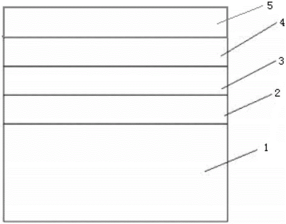
[0021] Such as figure 1 A multilayer passivation film for a crystalline silicon battery is shown, and the multilayer passivation film for a crystalline silicon battery is formed on a P-type crystalline silicon battery 1, which includes a first silicon oxide film 2, a silicon nitride film 3, a first Silicon dioxide film 4 and silicon nitride oxide film 5; silicon nitride film 3 is deposited on the first silicon oxide film 2; second silicon oxide film 4 is deposited on the silicon nitride film 3, and silicon nitride oxide film 5 is deposited on the second On the silicon dioxide film 4; th...


PUM

PropertyMeasurementUnit
Thicknessaaaaaaaaaa
Thicknessaaaaaaaaaa
Thicknessaaaaaaaaaa

Abstract

The invention discloses a multilayer passivation film of a crystalline-silicon battery and a manufacturing method thereof. The multilayer passivation film comprises a first silicon oxide film, a silicon nitride film, a second silicon oxide film and a silicon oxynitride film. The silicon nitride film is deposited on the first silicon oxide film; the second silicon oxide film is deposited on the silicon nitride film; and the silicon oxynitride film is deposited on the second silicon oxide film. The thickness of the first silicon oxide film is 5 to 9 nm, the thickness of the silicon nitride film is 60 to 90 nm, the thickness of the second silicon oxide film is 10 to 20nm, and the thickness of the silicon oxynitride film is 15 to 30nm. According to the invention, the probability of total reflection of light is improved substantially and thus more light enters a silicon wafer to generate more carriers, so that the battery efficiency is enhanced.

Description

technical field [0001] The invention relates to the technical field of solar cells, in particular to a multilayer passivation film for crystalline silicon cells and a manufacturing method thereof. Background technique [0002] At present, in the mass production of solar cells, anti-reflection coatings are often deposited on the surface of silicon wafers to increase light utilization and improve cell conversion efficiency. Common thin films mainly include silicon nitride SiNx and silicon oxide SiOx, and the two thin films have different characteristics and preparation methods. Silicon nitride SiNx films are mostly prepared by PECVD deposition, which has the characteristics of good anti-reflection performance, good bulk passivation effect, low deposition temperature, and high productivity, but the high bonding interface state and extinction characteristics of silicon nitride film and silicon substrate are also limited. The further improvement of the battery conversion efficie...

Claims


Application Information

Patent Timeline
IPC IPC(8): H01L31/0216H01L31/068H01L31/18
CPCH01L31/02167H01L31/02168H01L31/068H01L31/1868Y02E10/547Y02P70/50
Inventor 庞倩桃
Owner 庞倩桃
Learn More