A method of preparation of the array -based activated film that enhances the light catalytic effect
A photocatalytic and thin-film technology, which is applied in the direction of catalyst activation/preparation, chemical instruments and methods, physical/chemical process catalysts, etc. It can solve problems such as poor bonding between the film and the substrate, small active specific surface area of the film, and complex preparation process. , to achieve enhanced photocatalytic performance, stable photocatalytic activity, and simple preparation process
- Summary
- Abstract
- Description
- Claims
- Application Information
AI Technical Summary
Problems solved by technology
Method used
Image
Examples
Embodiment 1
[0026] The preparation method of the arrayed active film with strong photocatalytic effect in this embodiment, the steps are as follows:
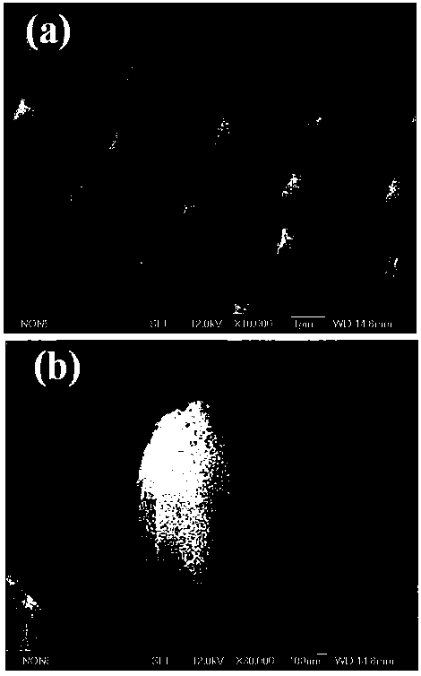
[0027] (1) A P-type monocrystalline silicon wafer with a resistivity of 0.015 Ω cm (the sample size is 2.5×2.5 cm 2 ) into the autoclave, and then fill the autoclave with corrosion solution, the corrosion solution is composed of hydrofluoric acid with a concentration of 8.00 mol / l and an aqueous ferric nitrate solution with a concentration of 0.08 mol / l, the solution in the autoclave The volume filling degree is 90%, and it is etched at 140°C for 35 minutes to prepare the substrate material silicon pillar array (Si-NPA). The scanning electron microscope shows figure 1 shown;
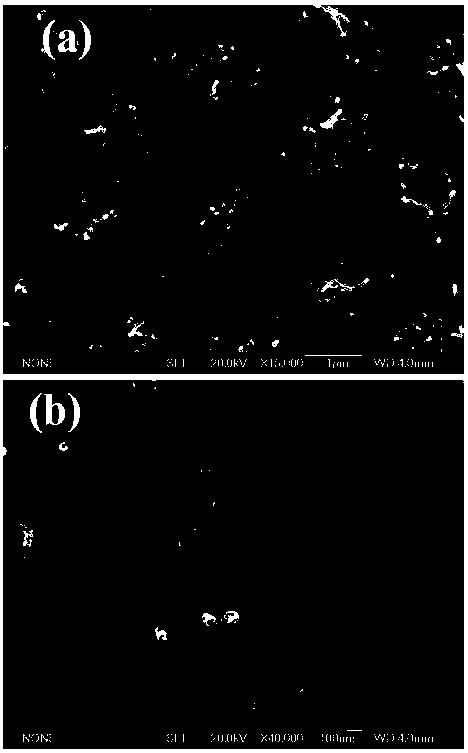
[0028] (2) Soak the silicon pillar array (Si-NPA) freshly prepared in step (1) in 0.002 mol / L ferrocene ethanol solution for 30 minutes, then place it in a horizontal tube furnace, and raise the temperature to The temperature was 760°C, and then ethylenediamine was ...
Embodiment 2
[0031] The preparation method of the arrayed active film with strong photocatalytic effect in this embodiment, the steps are as follows:
[0032] (1) A P-type monocrystalline silicon wafer with a resistivity of 0.03 Ωcm (the sample size is 2.5×2.5 cm 2 ) into the autoclave, and then fill the autoclave with corrosion solution. The corrosion solution is composed of hydrofluoric acid with a concentration of 8.00mol / l and an aqueous ferric nitrate solution with a concentration of 0.08 mol / l. The solution in the autoclave The volume filling degree is 90%, etched at 100°C for 40 min, and the substrate silicon pillar array (Si-NPA) is prepared;
[0033](2) Soak the silicon pillar array (Si-NPA) freshly prepared in step (1) in 0.002 mol / L ferrocene ethanol solution for 20 min, then place it in a horizontal tube furnace, nitrogen (60 sccm ) was heated to 800 °C under the protection of nitrogen gas, and then ethylenediamine was brought into the furnace at a rate of 1.5 mL / min to grow c...
Embodiment 3
[0036] The preparation method of the arrayed active film with strong photocatalytic effect in this embodiment, the steps are as follows:
[0037] (1) A P-type monocrystalline silicon wafer with a resistivity of 0.03 Ωcm (the sample size is 2.5×2.5 cm 2 ) into the autoclave, and then fill the autoclave with corrosion solution. The corrosion solution is composed of hydrofluoric acid with a concentration of 15.00mol / l and an aqueous ferric nitrate solution with a concentration of 0.02mol / l. The solution in the autoclave The volume filling degree is 90%, etched at 200°C for 30 min, and the substrate silicon pillar array (Si-NPA) is prepared;
[0038] (2) Soak the freshly prepared silicon pillar array (Si-NPA) in step (1) in 0.002 mol / L ferrocene ethanol solution for 25 min, then place it in a horizontal tube furnace, nitrogen (60 sccm ) to 780°C under the protection of nitrogen gas, then bring ethylenediamine into the furnace at 1.2 mL / min to grow carbon nanotubes in situ at 780°...
PUM
| Property | Measurement | Unit |
|---|---|---|
| electrical resistivity | aaaaa | aaaaa |
Abstract
Description
Claims
Application Information
 - R&D
- Intellectual Property
- Life Sciences
- Materials
- Tech Scout
- Unparalleled Data Quality
- Higher Quality Content
- 60% Fewer Hallucinations
Browse by: Latest US Patents, China's latest patents, Technical Efficacy Thesaurus, Application Domain, Technology Topic, Popular Technical Reports.
© 2025 PatSnap. All rights reserved.Legal|Privacy policy|Modern Slavery Act Transparency Statement|Sitemap|About US| Contact US: help@patsnap.com


