Memory cell used for SRAM (Static Random Access Memory) and read-write method thereof
A technology of storage unit and bit line, which is applied in the field of SRAM storage unit and its reading and writing, to achieve the effect of improving write tolerance, improving stability and solving stability
- Summary
- Abstract
- Description
- Claims
- Application Information
AI Technical Summary
Problems solved by technology
Method used
Image
Examples
Embodiment 1
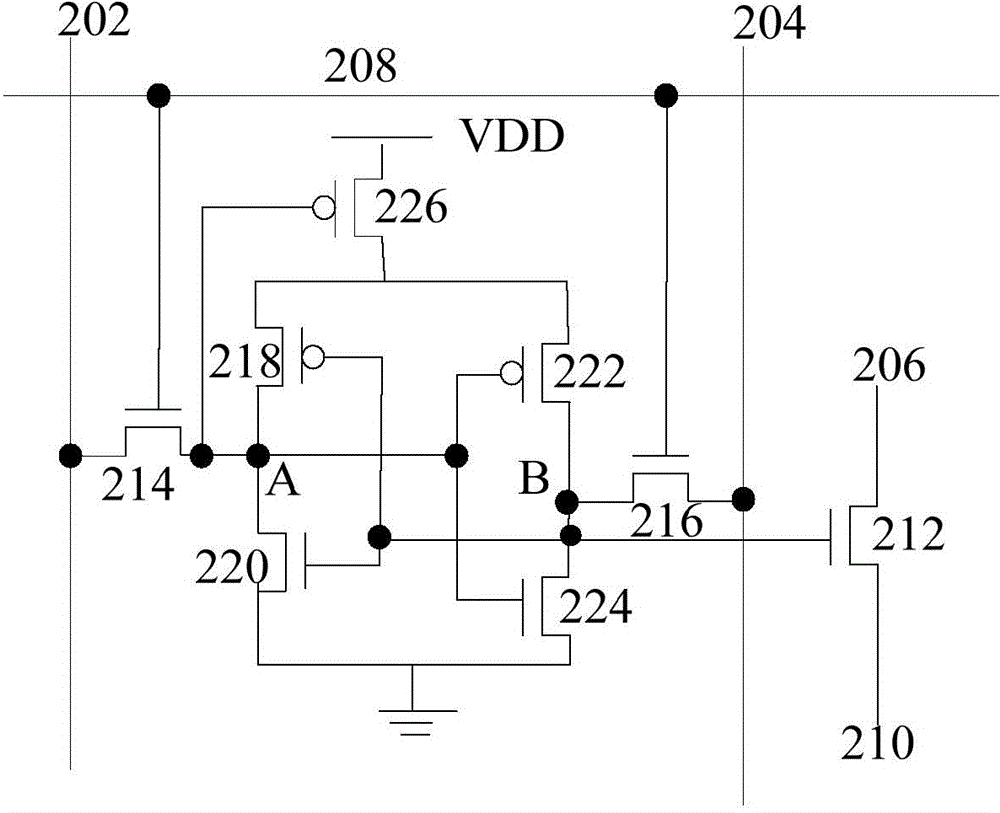
[0026] According to an embodiment of the present invention, a storage unit for SRAM is also provided, such as figure 2 As shown, the storage unit includes:
[0027] 1) The first bit line 202, the second bit line 204, the third bit line 206, the first word line 208 and the second word line 210, wherein the first word line 208 is used to control the memory cell written by the first word line The level state indicated by the bit line 202 and / or the second bit line 204, the second word line 210 is used to control the read level state from the memory cell, and the third bit line 206 is used to output the read level state;
[0028] 2) The first transistor 212 is connected between the third bit line 206 and the second word line 210 through the source and the drain, and is connected to the transistor group between the first bit line and the second bit line through the gate, and the transistor The group is used for writing the level states indicated by the first bit line and the sec...
Embodiment approach
[0033] 1) Read "1" operation: assume figure 2 Midpoint B stores data as "1", RBL is pre-charged to "1",
[0034] When RWL is currently "0", M7 is turned on, and the data "1" on point B is read through the line between M7 and point B. At this time, RBL maintains the voltage VDD state, and the signal is controlled by the amplifier SA connected to RBL. Amplify and read "1";
[0035] 2) Read "0" operation: assume figure 2 Midpoint B stores data as "0", RBL is pre-charged to "1",
[0036] When RWL is currently "0", M7 is turned on, and the data "0" on point B is read through the line between M7 and point B. At this time, RBL is discharged, and the signal is amplified and read by the amplifier SA connected to RBL. "0".
[0037] Here, when the read operation is performed, the RWL is "0" to indicate that it is at a low level, wherein the read operation can only be enabled when the RWL is set at a low level, that is, the read operation is triggered. because figure 2 The data sto...
Embodiment 2
[0064] According to an embodiment of the present invention, a method for reading a storage unit is provided for figure 2 shown in the memory cell, specifically as Figure 4 As shown, the method includes:
[0065] S402. Preset the third bit line to the first level;
[0066] S404, applying a second level to the second word line according to the first level;
[0067] S406, judging whether to read the level state stored in the storage unit according to the second level;
[0068] S408, if it is determined to read the level state stored in the memory cell, read out the stored level state from the third bit line.
[0069] Optionally, in this embodiment, the first level is a high level and the second level is a low level, or the first level is a low level and the second level is a high level.
[0070] Optionally, if it is determined to read the level state stored in the memory cell, then reading the stored level state by the third bit line includes:
[0071] S1, reading the leve...
PUM
 Abstract
Description
Claims
Application Information
 - R&D
- Intellectual Property
- Life Sciences
- Materials
- Tech Scout
- Unparalleled Data Quality
- Higher Quality Content
- 60% Fewer Hallucinations
Browse by: Latest US Patents, China's latest patents, Technical Efficacy Thesaurus, Application Domain, Technology Topic, Popular Technical Reports.
© 2025 PatSnap. All rights reserved.Legal|Privacy policy|Modern Slavery Act Transparency Statement|Sitemap|About US| Contact US: help@patsnap.com


