A chip package solid crystal solder paste and its preparation method and use process
A chip packaging and solid crystal technology, which is applied in manufacturing tools, metal processing, welding equipment, etc., can solve problems affecting chip welding strength, reduce interface thermal resistance, reduce packaging reliability, etc., and achieve excellent thermal stability and oxidation resistance properties, improved permeability and wettability, good fluidity and thermal conductivity
- Summary
- Abstract
- Description
- Claims
- Application Information
AI Technical Summary
Problems solved by technology
Method used
Image

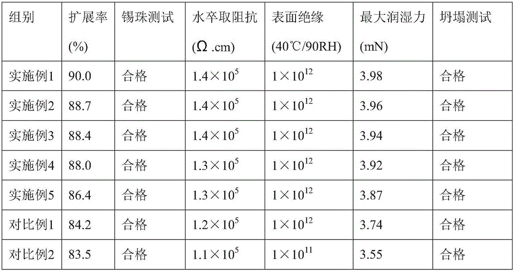
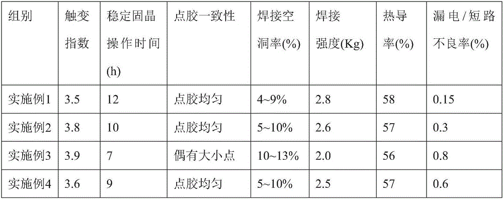
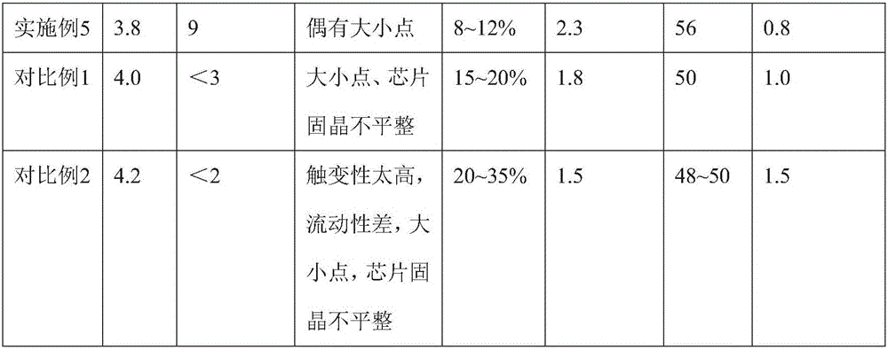
Examples
Embodiment 1
[0046] The crystal-fixing solder paste of Example 1 of the present invention consists of the following components in weight percent:
[0047] Sn96.5Ag3Cu0.582% and solder paste 18%;
[0048] Wherein, the solder paste is composed of the following components by weight percentage: rosin resin 25%, solvent 40%, dioctyl adipate 8%, ethylene bis stearic acid amide 3%, decyl myristate 4%, Rosin amine polyoxyethylene ether 8%, PLUS 2% and Pentaerythritol Cetate 10%;
[0049] Specifically, the rosin resin is composed of monoethyl maleopimarate and perhydrogenated rosin in a ratio of 1:2; the solvent is composed of isopropanol, carbitol and diethylene glycol butyl ether in a ratio of 1:3: The proportioning composition of 1;
[0050] Preparation:
[0051] (1) The solvent and the rosin resin are added to the reaction kettle in proportion to dissolve, the dissolution temperature is 90°C, and the stirring speed is 2500r / min;
[0052] (2) After the rosin resin is completely dissolved, ...
Embodiment 2
[0063] The crystal-fixing solder paste of Example 2 of the present invention consists of the following components in weight percent:
[0064] Sn96.5Ag3Cu0.582% and solder paste 18%;
[0065] Wherein, the solder paste is composed of the following components by weight percentage: rosin resin 20%, solvent 45%, dioctyl adipate 10%, ethylene bis stearic acid amide 4%, decyl tetradecyl tetradecanoic acid 2%, rosin amine polyoxyethylene ether 8%, PLUS 3% and Pentaerythritol Cetate 8%;
[0066] Specifically, the rosin resin is composed of monoethyl maleopimarate and perhydrogenated rosin in a ratio of 1:2; the solvent is composed of isopropanol, carbitol and diethylene glycol butyl ether in a ratio of 1:3: The proportioning composition of 1;
[0067] The preparation method and application process refer to Example 1, and the viscosity of the obtained die-bonding solder paste is 40pa.s.
Embodiment 3
[0069] The crystal-fixing solder paste of Example 3 of the present invention consists of the following components in weight percent:
[0070] Sn96.5Ag3Cu0.582% and solder paste 18%;
[0071] Wherein, the solder paste is composed of the following components by weight percentage: 30% rosin resin, 40% solvent, 6% dioctyl adipate, 4% ethylene bisstearic acid amide, decyl tetradecyl tetradecanoic acid 6%, rosin amine polyoxyethylene ether 6%, PLUS 3% and Pentaerythritol Cetate 5%;
[0072] Specifically, the rosin resin is composed of monoethyl maleopimarate and perhydrogenated rosin in a ratio of 1:2; the solvent is composed of isopropanol, carbitol and diethylene glycol butyl ether in a ratio of 1:3: The proportioning composition of 1;
[0073] The preparation method and application process refer to Example 1, and the viscosity of the obtained die-bonding solder paste is 40pa.s.
PUM
| Property | Measurement | Unit |
|---|---|---|
| particle diameter | aaaaa | aaaaa |
| particle diameter | aaaaa | aaaaa |
Abstract
Description
Claims
Application Information
 - R&D
- Intellectual Property
- Life Sciences
- Materials
- Tech Scout
- Unparalleled Data Quality
- Higher Quality Content
- 60% Fewer Hallucinations
Browse by: Latest US Patents, China's latest patents, Technical Efficacy Thesaurus, Application Domain, Technology Topic, Popular Technical Reports.
© 2025 PatSnap. All rights reserved.Legal|Privacy policy|Modern Slavery Act Transparency Statement|Sitemap|About US| Contact US: help@patsnap.com