SiC metal-oxide-semiconductor field-effect transistor (MOSFET) device and fabrication method thereof

A silicon carbide and device technology, which is applied in semiconductor/solid-state device manufacturing, semiconductor devices, electrical components, etc., can solve the problems of complex process flow and high manufacturing cost of SiC-based MOSFET devices

Active Publication Date: 2016-07-27
ZHEJIANG XINKE SEMICON CO LTD
View PDF4 Cites 19 Cited by
  • Summary
  • Abstract
  • Description
  • Claims
  • Application Information

AI Technical Summary

Problems solved by technology

[0005] The purpose of the present invention is to solve the problems of high manufacturing cost and complex process flow of SiC-based MOSFET devices.

Method used


Image

  • SiC metal-oxide-semiconductor field-effect transistor (MOSFET) device and fabrication method thereof
  • SiC metal-oxide-semiconductor field-effect transistor (MOSFET) device and fabrication method thereof
  • SiC metal-oxide-semiconductor field-effect transistor (MOSFET) device and fabrication method thereof

Examples


Embodiment Construction

[0041] The technical solution of the present invention is comprehensively considered from the aspects of device structure, device performance, process difficulty, and device cost, and reduces the total number of photoresist plates required for SiC MOSFET preparation to seven by multiplexing the photoresist plates, reducing the cost of device preparation. the cost of.

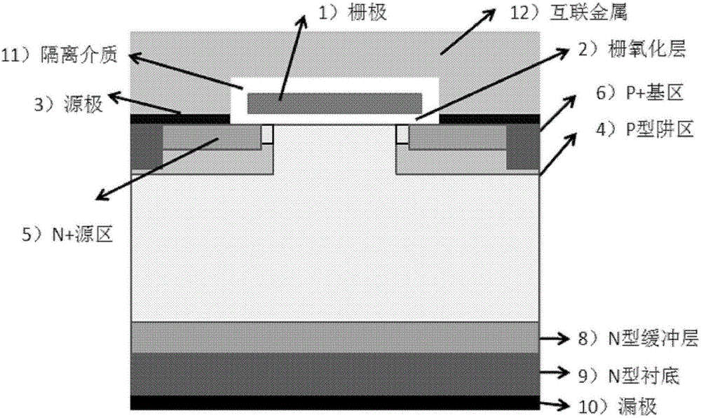
[0042] figure 1 is a schematic diagram of a single silicon carbide MOSFET cell structure according to the present invention. like figure 1 As shown, the SiC-based MOSFET device cell of the present invention includes: 1) a gate; 2) a gate oxide layer; 3) two sources; 4) two P-type well regions; 5) two N+ 6) Two P+ base regions; 7) An N-type drift layer; 8) An N+ buffer layer; 9) An N+ substrate; 10) Drain; 11) Isolation medium; 12) Interconnection metal.

[0043] Among them, the gate 1 and the source 3 are located on the front of the device, that is, on the (000) crystal plane of the epitaxial wafer, and the d...


PUM


Abstract

The invention discloses a SiC metal-oxide-semiconductor field-effect transistor (MOSFET) device and a fabrication method thereof. The SiC MOSFET device comprises a plurality of cells, wherein the cells are connected through interconnection metal (12), each cell comprises a grid, a grid oxide layer, two sources, an N-type drift layer, an N+ buffer layer, an N+ substrate, a drain and an isolation medium. According to the process step disclosed by the invention, in a photoetching plate subjected to tapping in a contact region, contact metal evaporation and stripping, a source electrode region is provided with a pattern, and a pattern also exists in a pad region of the grid.

Description

technical field [0001] The invention relates to the field of silicon carbide semiconductor device preparation, in particular to a silicon carbide MOSFET device and a preparation method thereof. The invention is a process method for optimizing the silicon carbide MOSFET preparation process. Background technique [0002] Silicon carbide (SiC) has excellent physical and electrical properties, wide band gap, high thermal conductivity, high breakdown field strength, high saturation electron drift rate, good chemical stability, strong radiation resistance and mechanical strength Etc. Therefore, SiC has become an ideal material for developing high-temperature, high-power, and high-frequency power devices, and has broad application prospects. SiC can generate silicon dioxide through thermal oxidation, so SiC materials can be used to prepare MOSFET devices with low on-resistance and high switching speed. [0003] Since the material cost and manufacturing cost of SiC-based power de...

Claims


Application Information

Patent Timeline
Patent Type & Authority Applications(China)
IPC IPC(8): H01L29/06H01L29/78H01L21/336
CPCH01L29/0684H01L29/66068H01L29/7827
Inventor 田丽欣温正欣张峰赵万顺王雷刘兴昉闫果果孙国胜曾一平
Owner ZHEJIANG XINKE SEMICON CO LTD
Why Eureka
Try Eureka