Antenna-integrated package structure and manufacturing method thereof

A technology of packaging structure and manufacturing method, which is applied in the direction of antenna support/mounting device, radiation element structure, etc., can solve the problems of substrate shrinkage manufacturing process efficiency, low assembly yield, and insufficient, so as to avoid high-frequency parasitic effects, Effect of reducing signal transmission loss and reducing signal transmission distance

Active Publication Date: 2019-01-04
IND TECH RES INST
View PDF5 Cites 0 Cited by
  • Summary
  • Abstract
  • Description
  • Claims
  • Application Information

AI Technical Summary

Problems solved by technology

Academic circles and major manufacturers at home and abroad have also successively developed chips in the millimeter wave frequency band; however, there is no complete solution for the packaging of chips in this frequency band
[0003] Traditional wire-bond packaging is not suitable for RF chip packaging, while using low-temperature co-fired multilayer ceramics (Low-Temperature Co-fired Ceramics, LTCC) and flip-chip packaging, the substrate shrinks due to the manufacturing process conditions and the production Insufficient process efficiency, coupled with the small pad size and pitch of the chip to be packaged, resulting in low assembly yield

Method used


Image

  • Antenna-integrated package structure and manufacturing method thereof
  • Antenna-integrated package structure and manufacturing method thereof
  • Antenna-integrated package structure and manufacturing method thereof

Examples


Embodiment Construction

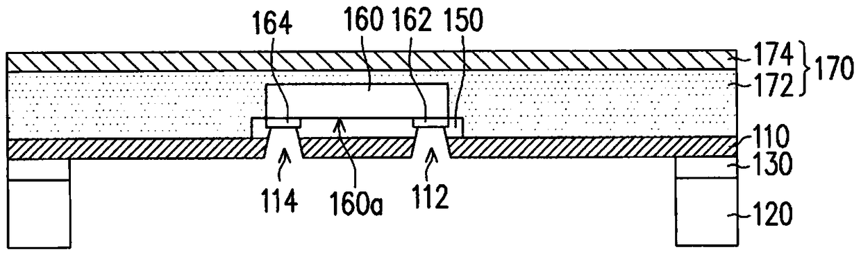
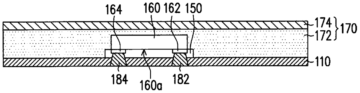
[0057] Figure 1 to Figure 6 It is a cross-sectional flowchart of a method for manufacturing an antenna-integrated package structure according to an embodiment of the present invention.

[0058] refer to figure 1 , first provide a carrier board 120 . Next, the first metal layer 110 is bonded to the carrier 120 , and the first metal layer 110 is bonded to the carrier 120 through the adhesive layer 130 . The bonding surface of the first metal layer 110 may have a release layer 140, the release layer 140 only partially covers the bonding surface, and in some areas the first metal layer 110 is bonded to the bonding surface through the release layer 140 and the adhesive layer 130. carrier plate 120 .

[0059] see figure 1, and then, a primer 150 is formed on the first metal layer 110 . A chip 160 is disposed on the primer 150 so that the chip 160 is attached to the first metal layer 110 through the primer 150 . The chip 160 has an active surface 160a, a first contact pad 162...


PUM


Abstract

The invention discloses an antenna integrated package structure and a fabrication method thereof. The package structure comprises a lamination structure and a multi-layer substrate, wherein the lamination structure comprises at least one chip and at least one plated via and through hole structure, the chip is buried in the lamination structure, the plated via and through hole structure passes through the lamination structure, the multi-layer substrate is laminated on the lamination structure and at least comprises a metal layer, the metal layer is arranged on one side, far away from the lamination structure, of the multi-layer substrate and at least comprises an antenna pattern, the antenna pattern is arranged above the chip, the multi-layer substrate comprises the plated via and through hole structure, the plated via and through hole structure passes through the multi-layer substrate and is connected with the plated via and through hole structure so as to electrically connect the antenna pattern and the chip. The invention also provides the fabrication method of the above antenna integrated package structure.

Description

technical field [0001] The present invention relates to a packaging structure and a manufacturing method thereof, and in particular to an antenna-integrated packaging structure and a manufacturing method thereof. Background technique [0002] The application of wireless receivers has become the focus of the CES in the past two years, announcing the advent of the era of Wireless Gigabit Alliance (WiGi) and Wireless High Definition (Wireless HD) standard applications. Academic circles and major manufacturers at home and abroad have also successively developed chips in the millimeter wave frequency band; however, there is no complete solution for the packaging of chips in this frequency band. [0003] Traditional wire-bond packaging is not suitable for RF chip packaging, while using low-temperature co-fired multilayer ceramics (Low-Temperature Co-fired Ceramics, LTCC) and flip-chip packaging, the substrate shrinks due to manufacturing process conditions and the production Insu...

Claims


Application Information

Patent Timeline
Patent Type & Authority Patents(China)
IPC IPC(8): H01Q1/38H01Q1/22
Inventor 蔡承桦钟世忠
Owner IND TECH RES INST
Why Eureka
Try Eureka