A kind of fcqfn package for preventing solder ball from collapsing and its manufacturing process

A manufacturing process and packaging technology, which is applied in semiconductor/solid-state device manufacturing, electrical components, electrical solid-state devices, etc. It can solve problems such as voids in plastic packaging materials, reduction of chips and frames, and impact on product reliability.

Active Publication Date: 2018-04-06
HUATIAN TECH XIAN
View PDF4 Cites 0 Cited by
  • Summary
  • Abstract
  • Description
  • Claims
  • Application Information

AI Technical Summary

Problems solved by technology

However, due to the limitations of traditional packaging in the past, the chip bumps melted and collapsed during the reflow process, causing a short circuit between the two chip bumps due to tin connection, and the height between the chip and the frame will also be reduced due to the collapse. Insufficient is likely to cause voids and affect product reliability

Method used


Image

  • A kind of fcqfn package for preventing solder ball from collapsing and its manufacturing process
  • A kind of fcqfn package for preventing solder ball from collapsing and its manufacturing process
  • A kind of fcqfn package for preventing solder ball from collapsing and its manufacturing process

Examples


Embodiment Construction

[0020] The present invention will be described in further detail below in conjunction with the accompanying drawings.

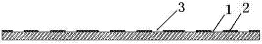
[0021] Such as Picture 11 As shown, an FCQFN package for preventing solder ball collapse is mainly composed of a copper lead frame 1, a first layer of green paint 2, a green paint groove 3, a chip 4, a tin-silver-copper bump 5, a plastic package body 6, and an etching The pin 8, the second layer of green paint 9 and the solder ball 10. The copper lead frame 1 is coated with a first layer of green paint 2, the first layer of green paint 2 has a green paint groove 3, and the green paint groove 3 is bonded with tin, silver, copper bumps 5 and chips 4. The plastic package 6 surrounds the upper surface of the copper lead frame 1, the first layer of green paint 2, the green paint groove 3, the chip 4, and the tin-silver-copper bumps 5, and forms the entire circuit. The etched pins 8 are formed by the etched copper lead frame 1. The etched copper lead frame 1 includ...


PUM

PropertyMeasurementUnit
thicknessaaaaaaaaaa
thicknessaaaaaaaaaa
diameteraaaaaaaaaa

Abstract

The invention discloses an FCQFN encapsulation part preventing solder balls from collapsing and a manufacturing process of the FCQFN encapsulation part. The encapsulation part is mainly composed of a copper lead frame, a first green paint layer, green paint grooves, chips, tin-silver-copper protruded points, a plastic packaging body, etched pins, a second green paint layer and the solder balls. The first green paint layer coats the copper lead frame and is provided with the green paint grooves, and the chips and the tin-silver-copper protruded points are adhered to the green paint grooves. The plastic packaging body wraps the upper surface of the copper lead frame, the first green paint layer, the green paint grooves, the chips and the tin-silver-copper protruded points to form an overall circuit. The etched pins are formed by the etched copper lead frame, the etched copper lead frame comprises an etching thinning area, the second green paint layer coats the inside of the etching thinning area, and the solder balls are located on the etched pins. The manufacturing process comprises the following steps of wafer thinning, wafer scribing, green paint coating of the frame, exposure development, inverse chip assembly, backflow cleaning, plastic packaging, thinning of the back face of the frame, etching and separation of the pins, green paint filling, steel mesh printing and ball mounting, cutting, packaging and delivery. According to the FCQFN encapsulation part preventing the solder balls from collapsing and the manufacturing process of the FCQFN encapsulation part, short circuit is prevented, filling performance of plastic packaging materials is improved, and therefore product reliability is promoted.

Description

Technical field [0001] The invention relates to the technical field of electronic information automation components manufacturing, in particular to an FCQFN package capable of preventing solder ball collapse and its manufacturing process. Background technique [0002] Flip Chip is not only a chip interconnection technology, but also an ideal chip bonding technology. As early as 30 years ago, IBM has developed and used this technology. But until recent years, Flip-Chip has become a packaging form often used in the field of high-end devices and high-density packaging. Today, the application range of Flip-Chip packaging technology is becoming wider and wider, and the packaging forms are becoming more diversified. The requirements for Flip-Chip packaging technology are also increasing. At the same time, Flip-Chip also poses a series of new severe challenges to manufacturers to provide reliable support for packaging, assembly and testing of this complex technology. In the past, the...

Claims


Application Information

Patent Timeline
Patent Type & Authority Patents(China)
IPC IPC(8): H01L23/495H01L21/60
CPCH01L24/97H01L2224/16H01L2924/15747H01L2924/00
Inventor 谌世广朱文辉刘卫东钟环清谢天禹
Owner HUATIAN TECH XIAN
Why Eureka
Try Eureka