Method for interconnecting and packaging 3-D multi-chip module

A multi-chip module and packaging method technology, applied in the field of microelectronics, can solve problems such as long signal delay time, long interconnection lines, and difficult assembly, so as to improve the speed of operation, reduce size and weight, and reduce volume and weight Effect

Inactive Publication Date: 2008-08-06
CHINA AEROSPACE TIMES ELECTRONICS CORP NO 771 RES INST
View PDF5 Cites 0 Cited by
  • Summary
  • Abstract
  • Description
  • Claims
  • Application Information

AI Technical Summary

Problems solved by technology

[0005] 1) The interconnection line between the MCM laminated module and the shell is long, the signal delay is obvious, and the reliability is low
[0006] 2) The manufacturing process of bumps is complicated, the cost is high, and the detection of solder joints is difficult
[0008] 4) The chip is vulnerable to stress damage
[0009] 5) Three-dimensional packaging has large volume and low mechanical strength
With this electrical interconnection method, the substrate size is relatively small, the thermal resistance is large, the assembly is difficult, and a special case needs to be developed
[0011] For a 2D laminated module with dimensions of 60mm×60mm×8mm ( figure 1 , figure 2 ), if the lead wire is directly used for interconnection, the length of the interconnection wire is very large (about 12mm), the signal delay time is long, and the reliability is low

Method used


Image

  • Method for interconnecting and packaging 3-D multi-chip module
  • Method for interconnecting and packaging 3-D multi-chip module
  • Method for interconnecting and packaging 3-D multi-chip module

Examples


Embodiment Construction

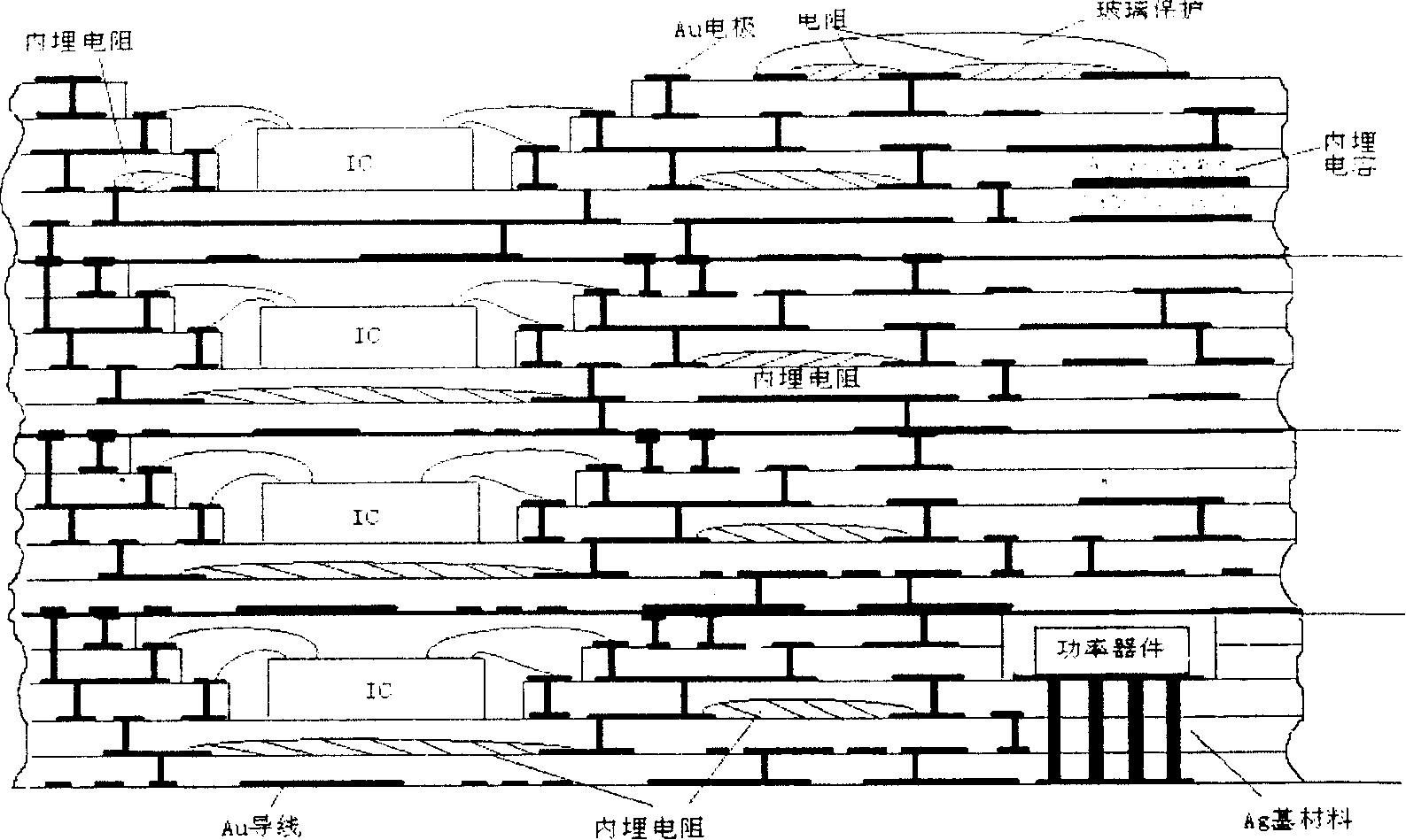
[0045] The 3D-MCM interconnection and packaging method is a key technology in 3D packaging. The three-dimensional multi-chip module interconnection and packaging method of the present invention includes the following content:

[0046] 1. Design of the back-shaped transition wiring substrate under the laminated module

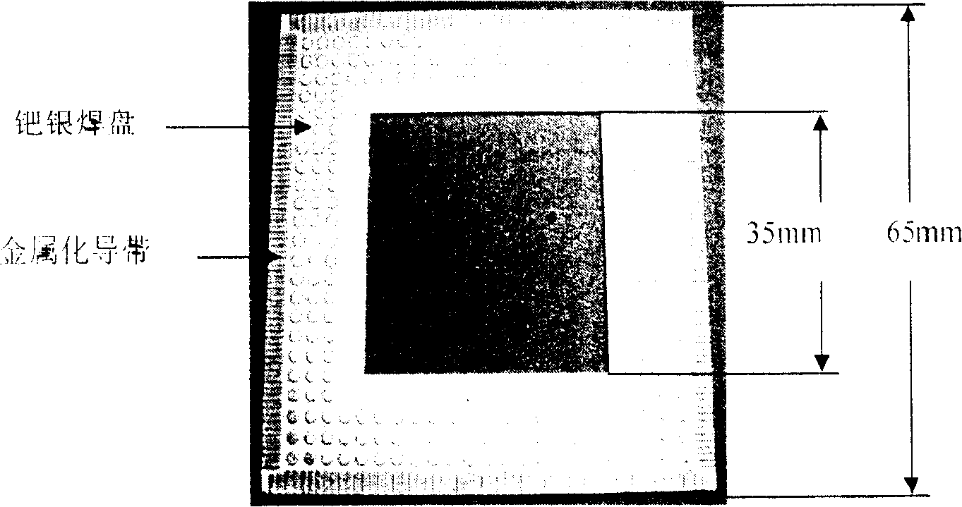
[0047] By scanning the metallization pattern under the MCM laminated module, the position and size of the metallized pad for vertical interconnection under the MCM laminated module can be accurately measured, avoiding the deformation and size error of the LTCC substrate due to sintering ;According to the above data, the size of the opening in the middle of the back-shaped transition wiring substrate and the specific position of the metallized pad can be clarified; by screen printing the palladium-silver paste, the MCM laminated module will be formed on the inside of the back-shaped transition wiring substrate The metallized interconnection patterns on the bottom...


PUM


Abstract

The invention discloses a 3D multichip module (MCM) interconnecting and packaging method, adopting ceramic bushing stacked transition wiring substrate to interconnect and package MCM stacked module, reducing system bulk and weight by various high density assembly to adapt to the development requirements of weapon equipment for miniaturization, high performance, multifunction, high reliability and low cost of electronic systems, converting the electronic packaging concept from device orientation into system orientation, thus increasing operational rate, assembling efficiency and heat radiating ability on the premise of assuring reliability and besides, increasing I / O number, reducing size and weight and cost. And the technical indexes of computer miniaturization by the method: operating frequency 25Mhz; connecting point number per unit area >or=104 / dm2; thermal resistance <0.45DEG C / W; I / O number 256; underfilling distance 30mm; and assembling efficiency 121%.

Description

technical field [0001] The invention belongs to the technical field of microelectronics and relates to the structural design of three-dimensional packaging, vertical interconnection, production of bumps and stacking reinforcement technology, specifically, a method for interconnection and packaging of three-dimensional multi-chip modules. Background technique [0002] Three-dimensional multi-chip module (3D-MCM) can effectively reduce the interconnection distance, interconnection resistance, interconnection capacitance and inductance of IC chips due to the use of vertical interconnection technology, which can reduce the transmission delay of signals by more than 300%. The assembly efficiency reaches more than 200%, which can further realize smaller volume and more functions, and has been developed rapidly at home and abroad. The structure of three-dimensional MCM is various. In terms of packaging structure, it can be divided into three categories: one is embedded 3D-MCM; the ...

Claims


Application Information

Patent Timeline
Patent Type & Authority Patents(China)
IPC IPC(8): H01L21/50
CPCH01L2224/45144H01L2224/48091H01L2224/48227H01L2224/49109H01L2924/00014H01L2924/00
Inventor 任爱华
Owner CHINA AEROSPACE TIMES ELECTRONICS CORP NO 771 RES INST
Why Eureka
Try Eureka