AINGaN base field effect transistor of high quality MIS structure and manufacturing method thereof
A MIS structure, high-quality technology, applied in semiconductor/solid-state device manufacturing, semiconductor devices, electrical components, etc., can solve the problem of high interface state density and gate dielectric layer of MIS interface system, poor quality of GaNMIS interface, affecting device stability and other problems, to achieve the effects of reduced MIS interface state density, high process repeatability and reliability, and high threshold voltage stability
- Summary
- Abstract
- Description
- Claims
- Application Information
AI Technical Summary
Problems solved by technology
Method used
Image

Examples
Embodiment 1
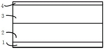
[0037] Such as Figure 11 Shown is a schematic diagram of the device structure of this embodiment, and its structure includes a substrate 1, a stress buffer layer 2, a GaN epitaxial layer 3, an AlN epitaxial layer 4, a secondary epitaxial layer 5, and grooves formed by secondary epitaxy from bottom to top. , a gate dielectric layer 6, a source 7 and a drain 8 are formed at both ends, and the dielectric layer 6 at the groove channel is covered with a gate 9.
[0038] The fabrication method of the GaN-based field-effect transistor of the above-mentioned high-quality MIS structure is as follows: Figure 1-Figure 11 shown, including the following steps:
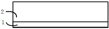
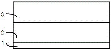
[0039] S1. Using the metal organic chemical vapor deposition method, grow a stress buffer layer (2) on the Si substrate (1), such as figure 1 shown;
[0040] S2. Using a metal organic chemical vapor deposition method to grow a GaN epitaxial layer (3) on the stress buffer layer (2), such as figure 2 shown;
[0041] S3. Usin...
Embodiment 2
[0052] Such as Figure 12 Shown is a schematic diagram of the device structure of this embodiment, which differs from the structure of Embodiment 1 only in that the GaN / AlGaN heterostructure in Embodiment 1 is formed by secondary epitaxy and a gate groove region is naturally formed at the same time, while in Embodiment 2 The structure of the secondary epitaxy is only AlGaN, and at the same time, the gate groove area is formed, and the number 11 is the AlGaN structure layer.
PUM
| Property | Measurement | Unit |
|---|---|---|
| Thickness | aaaaa | aaaaa |
| Thickness | aaaaa | aaaaa |
| Thickness | aaaaa | aaaaa |
Abstract
Description
Claims
Application Information
 - R&D
- Intellectual Property
- Life Sciences
- Materials
- Tech Scout
- Unparalleled Data Quality
- Higher Quality Content
- 60% Fewer Hallucinations
Browse by: Latest US Patents, China's latest patents, Technical Efficacy Thesaurus, Application Domain, Technology Topic, Popular Technical Reports.
© 2025 PatSnap. All rights reserved.Legal|Privacy policy|Modern Slavery Act Transparency Statement|Sitemap|About US| Contact US: help@patsnap.com