
Reading-out amplifier and MRAM (Magnetic Random Access Memory) chip

A readout amplifier and chip technology, applied in the direction of instruments, static memory, digital memory information, etc., can solve the problem of unable to break through the speed bottleneck, and achieve the effect of improving the yield rate of MRAM chips, saving power in readout operations, and fast speed

Active Publication Date: 2016-07-13
SHANGHAI CIYU INFORMATION TECH
View PDF5 Cites 9 Cited by
  • Summary
  • Abstract
  • Description
  • Claims
  • Application Information

AI Technical Summary

Problems solved by technology

This is the main factor that restricts the reading speed. Most of the time for reading memory data is spent charging this parasitic capacitance, and the time is about Δt=2C b R m , this design cannot break through this speed bottleneck

Method used


Image

  • Reading-out amplifier and MRAM (Magnetic Random Access Memory) chip
  • Reading-out amplifier and MRAM (Magnetic Random Access Memory) chip
  • Reading-out amplifier and MRAM (Magnetic Random Access Memory) chip

Examples


Embodiment Construction

[0055] The present invention relates to a sense amplifier, comprising an input part and a differential current output part, the input part and the differential current output part are connected at the first input terminal V_in and the second input terminal V_in_n of the input part; wherein, the first The input terminal V_in is used to input the current passing through the storage unit, and the second input terminal V_in_n is used to input the current passing through the reference unit; the differential current output part is used to compare the two currents input by the input part and output the comparison result.

[0056] Such as Image 6 As shown, the sense amplifier includes an input part and a differential current output part, and the input part and the differential current output part are connected at the first input terminal V_in and the second input terminal V_in_n.

[0057] The differential current output part includes a P-type MOS transistor P0, a P-type MOS transisto...


PUM


Abstract

The invention provides a reading-out amplifier. The reading-out amplifier comprises an input part and a differential current output part, wherein the input part and the differential current output part are connected at a first input end V_in and a second input end V_in_n of the input part; the first input end V_in is used for inputting current passing through a storage unit; the second input end V_in_n is used for inputting current passing through a reference unit; the differential current output part is used for comparing two currents input by the input part and outputting a comparing result. The invention further provides an MRAM (Magnetic Random Access Memory) chip. According to the reading-out amplifier and the MRAM chip, provided by the invention, the resistance is optimal, so that the reading-out speed is rapider and reading-out operation saves more power; the distribution of reference resistance becomes narrow, the fault probability for judging a high-resistance state and a low-resistance state is reduced and the yield of the MRAM chip is improved; parameters are selected so that the resistance of a combined reference unit is mostly close to an optimal selection, and furthermore, the yield of the MRAM chip is improved.

Description

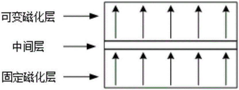
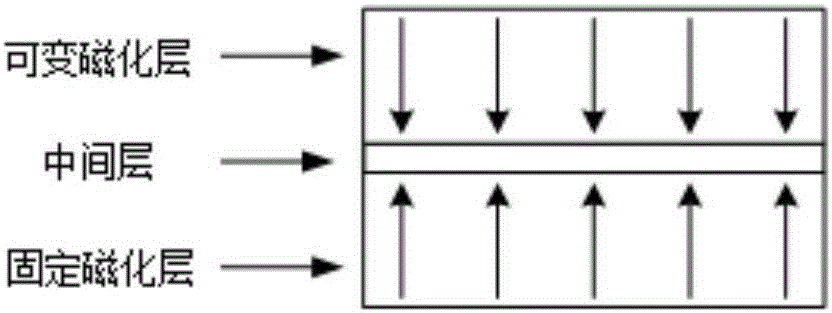
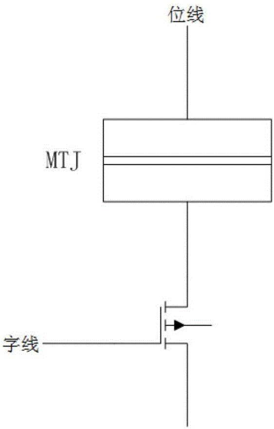
technical field [0001] The invention relates to the field of semiconductor chips, in particular to a sense amplifier and an MRAM chip. Background technique [0002] About MRAMs: [0003] The background of the present invention is the maturity of MRAM technology. MRAM is a new memory and storage technology that can be read and written as fast as SRAM / DRAM, and can permanently retain data after power failure like Flash memory. [0004] The economy of MRAM is quite good, and the area of ​​silicon chip occupied per unit capacity has a great advantage over SRAM, and also has advantages over NORFlash, which is often used in such chips, and has greater advantages than embedded NORFlash. The performance of MRAM is also quite good, the read and write delay is close to the best SRAM, and the power consumption is the best among various memory and storage technologies. Moreover, MRAM is not compatible with standard CMOS semiconductor processes like DRAM and Flash. MRAM can be integr...

Claims


Application Information

Patent Timeline
IPC IPC(8): G11C11/16
CPCG11C11/1673G11C11/16
Inventor 戴瑾
Owner SHANGHAI CIYU INFORMATION TECH
Learn More