CMOS driver wafer level package and manufacturing method thereof
A technology of wafer-level packaging and manufacturing method, applied in semiconductor/solid-state device manufacturing, electric solid-state devices, semiconductor devices, etc., can solve problems affecting the performance of driver chips, achieve stable and reliable electrical connection, reduce parasitic inductance and Parasitic capacitance effect, performance improvement effect
- Summary
- Abstract
- Description
- Claims
- Application Information
AI Technical Summary
Problems solved by technology
Method used
Image
Examples
Embodiment 1
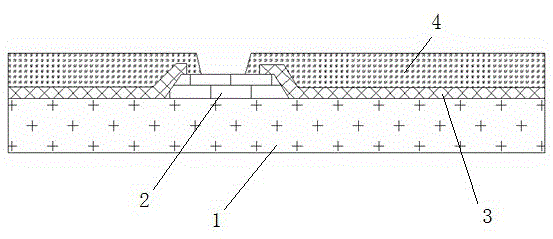
[0029] like Figure 5 As shown, the present invention discloses a CMOS driver wafer-level package, including a driver wafer 1, a driver wafer bonding pad 2 is formed on the upper surface part of the wafer, and the area outside the bonding pad area A passivation layer 3 is formed on the upper surface of the wafer, a first resin layer 4 is formed on the upper surface of the passivation layer 3, and the inner edge of the first resin layer 4 extends to the upper surface of the pad, Part of the upper surface of the pad is covered by the first resin layer 4 , and the rest is exposed. Preferably, the first resin layer 4 is made of polyimide material.
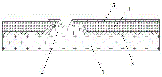
[0030] Part of the upper surface of the first resin layer 4 is formed with a rewiring layer 5, and part of the rewiring layer 5 is in direct contact with the exposed part of the upper surface of the pad; the upper surface of the rewiring layer 5 is not covered The upper surface of the first resin layer 4 of the rewiring layer 5 is for...
Embodiment 2
[0032] The invention also discloses a method for manufacturing a CMOS driver wafer-level package, comprising the following steps:
[0033] 1) Take a driver wafer and clean the surface of the wafer.
[0034] 2) Deposit the passivation layer 3 and the first resin layer 4 sequentially on the upper surface of the driver wafer 1, and etch the passivation layer 3 and the first resin layer 4 to etch the driver wafer pad area , and then form the driver wafer bonding pad 2 in the above region, preferably, the first resin layer is made of polyimide material, such as figure 1 shown;
[0035] 3) sputtering or depositing a rewiring layer 5 on part of the upper surface of the above-mentioned device, so that the rewiring layer 5 part is in contact with the driver wafer pad 2, as figure 2 shown;
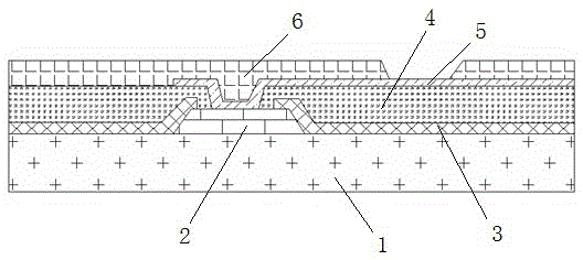
[0036] 4) Depositing the second resin layer 6 on the rewiring layer 5, etching the second resin layer 6, so that part of the rewiring layer 5 is exposed, and then etching the exposed part of the...
PUM
| Property | Measurement | Unit |
|---|---|---|
| Diameter | aaaaa | aaaaa |
Abstract
Description
Claims
Application Information
 - R&D
- Intellectual Property
- Life Sciences
- Materials
- Tech Scout
- Unparalleled Data Quality
- Higher Quality Content
- 60% Fewer Hallucinations
Browse by: Latest US Patents, China's latest patents, Technical Efficacy Thesaurus, Application Domain, Technology Topic, Popular Technical Reports.
© 2025 PatSnap. All rights reserved.Legal|Privacy policy|Modern Slavery Act Transparency Statement|Sitemap|About US| Contact US: help@patsnap.com


