SiC-based diluted magnetic semiconductor thin film and preparation method thereof
A technology of dilute magnetic semiconductor and thin film, applied in the direction of magnetic thin film, magnetic object, magnetic material, etc., can solve the problem of weak dilute magnetic strength of SiC material, and achieve the effect of stable and effective method, good application value and strong saturation magnetization
- Summary
- Abstract
- Description
- Claims
- Application Information
AI Technical Summary
Problems solved by technology
Method used
Image
Examples
Embodiment 1
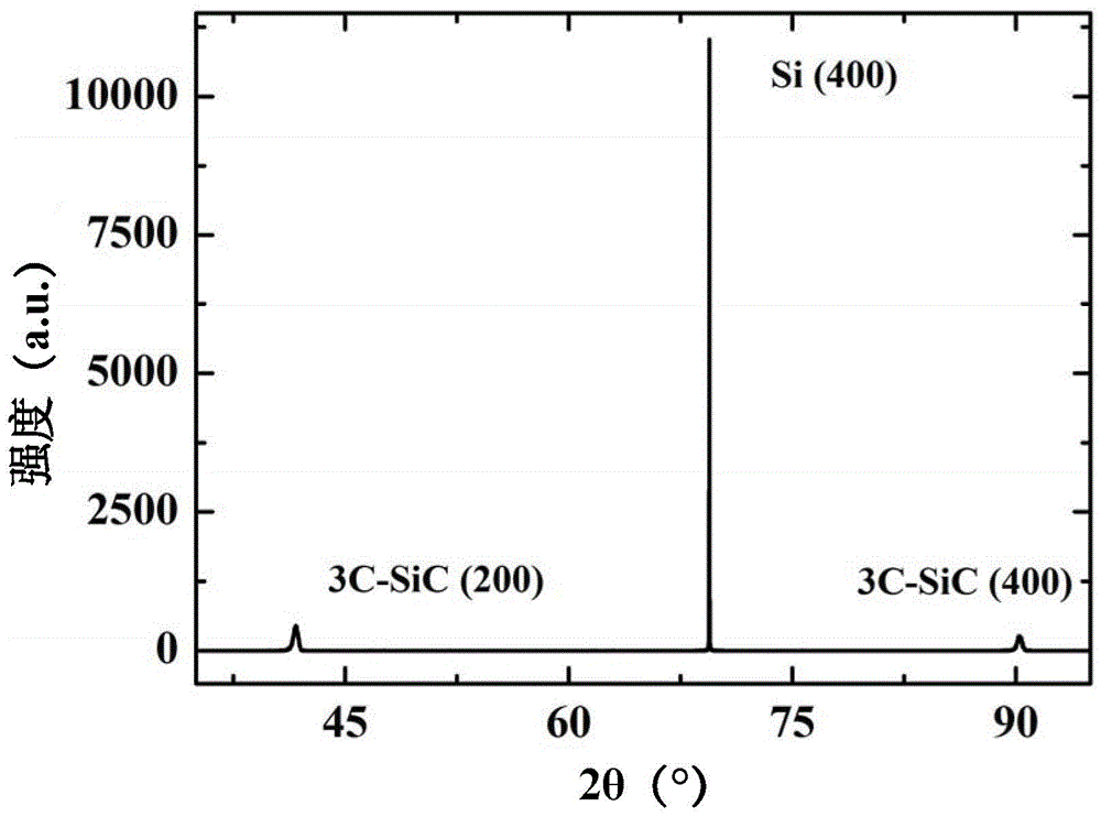
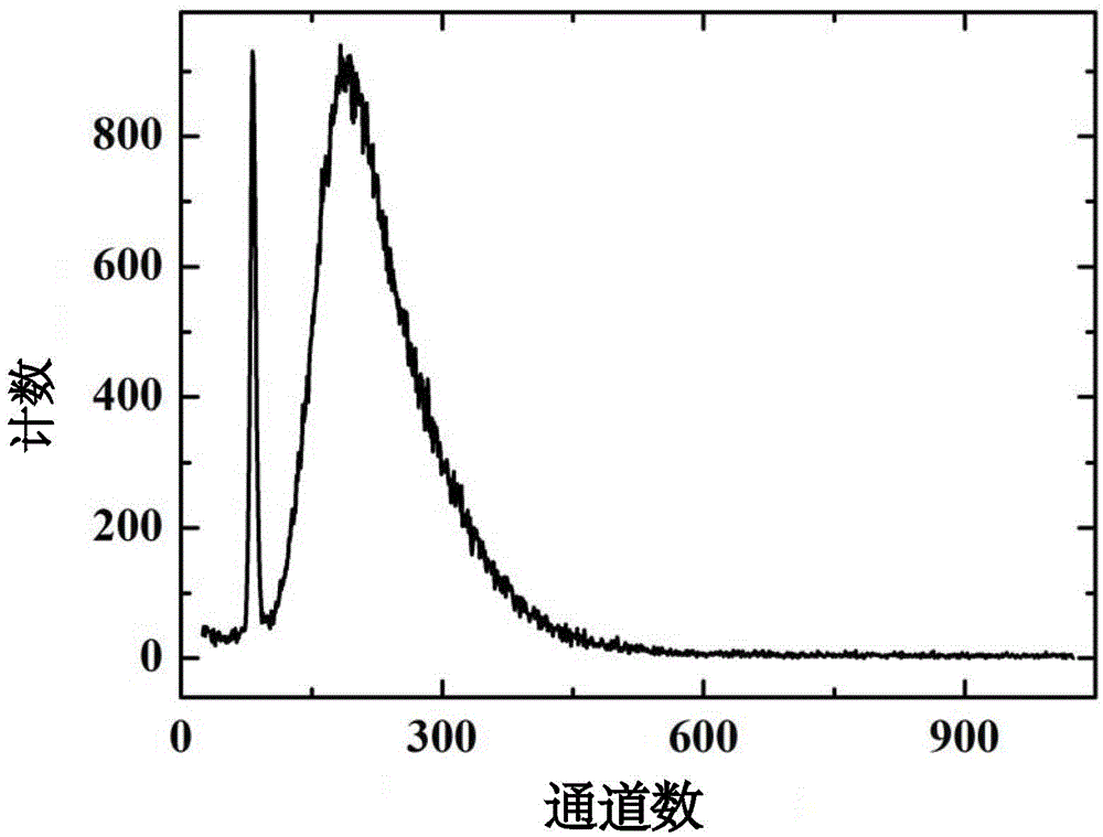
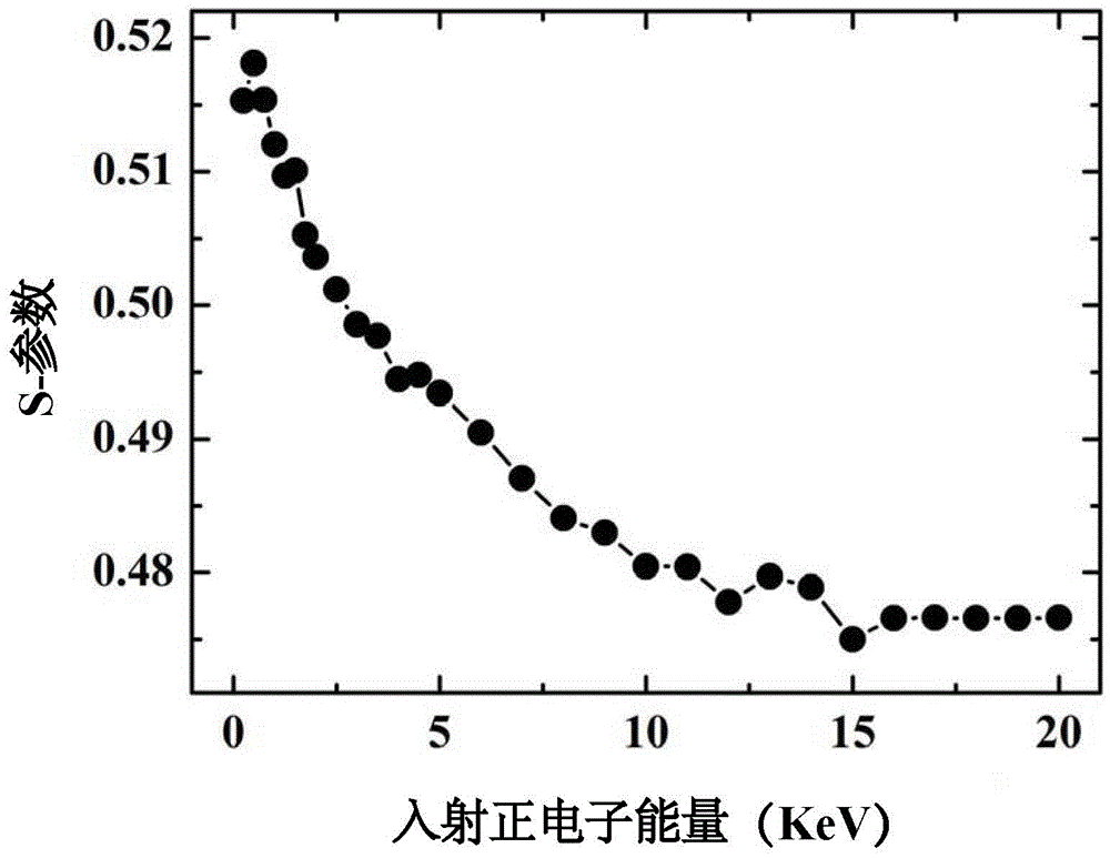
[0045] (1) Put the silicon substrate into a mixed solution of ammonia water: hydrogen peroxide: deionized water = 1:1:5 to clean for 15 minutes, and then rinse with deionized water for 10 minutes; (2) Put the silicon substrate into hydrochloric acid: hydrogen peroxide: Wash in the mixed solution of deionized water=1:1:5 for 15min, then rinse with deionized water for 10min; (3) wash the silicon substrate with high-purity N 2 Blow dry; (4) Put the silicon substrate, graphite plate, and quartz boat into the quartz cavity; (5) Pump the quartz cavity to a background vacuum of ≤5.0×10 -4 Pa, rush into 2slm hydrogen to normal pressure; (6) turn on the intermediate frequency radio frequency power supply, pass into H 2 :HCl=1:0.5% mixed gas at 1020°C for 5 minutes; (7) After the etching is completed, cut into H 2 :C 3 h 8 =1:0.045% mixed gas at 1200°C for 10 minutes; (8) After carbonization is completed, the temperature is directly raised to 1350°C, and HCl:SiH4=1:0.08%, C / Si=3.2 ga...
Embodiment 2
[0047] (1) Put the silicon substrate into a mixed solution of ammonia water: hydrogen peroxide: deionized water = 1:1:5 to clean for 15 minutes, and then rinse with deionized water for 10 minutes; (2) Put the silicon substrate into hydrochloric acid: hydrogen peroxide: Wash in the mixed solution of deionized water=1:1:5 for 15min, then rinse with deionized water for 10min; (3) wash the silicon substrate with high-purity N 2 Blow dry; (4) Put the silicon substrate, graphite plate, and quartz boat into the quartz cavity; (5) Pump the quartz cavity to a background vacuum of ≤5.0×10 -4 Pa, rush into 2slm hydrogen to normal pressure; (6) turn on the intermediate frequency radio frequency power supply, pass into H 2 :HCl=1:0.5% mixed gas at 1020°C for 5 minutes; (7) After the etching is completed, cut into H 2 :C 3 h 8 =1:0.045% mixed gas at 1200°C for 10 minutes; (8) After carbonization is completed, the temperature is directly raised to 1350°C, and HCl:SiH4=1:0.08%, C / Si=3.2 ga...
Embodiment 3
[0049] (1) Put the silicon substrate into a mixed solution of ammonia water: hydrogen peroxide: deionized water = 1:1:5 to clean for 15 minutes, and then rinse with deionized water for 10 minutes; (2) Put the silicon substrate into hydrochloric acid: hydrogen peroxide: Wash in the mixed solution of deionized water=1:1:5 for 15min, then rinse with deionized water for 10min; (3) wash the silicon substrate with high-purity N 2 Blow dry; (4) Put the silicon substrate, graphite plate, and quartz boat into the quartz cavity; (5) Pump the quartz cavity to a background vacuum of ≤5.0×10 -4 Pa, rush into 2slm hydrogen to normal pressure; (6) turn on the intermediate frequency radio frequency power supply, pass into H 2 :HCl=1:0.5% mixed gas at 1020°C for 5 minutes; (7) After the etching is completed, cut into H 2 :C 3 h 8 =1:0.045% mixed gas at 1200°C for 10 minutes; (8) After carbonization is completed, the temperature is directly raised to 1350°C, and HCl:SiH4=1:0.08%, C / Si=3.2 ga...
PUM
 Abstract
Description
Claims
Application Information
 - R&D
- Intellectual Property
- Life Sciences
- Materials
- Tech Scout
- Unparalleled Data Quality
- Higher Quality Content
- 60% Fewer Hallucinations
Browse by: Latest US Patents, China's latest patents, Technical Efficacy Thesaurus, Application Domain, Technology Topic, Popular Technical Reports.
© 2025 PatSnap. All rights reserved.Legal|Privacy policy|Modern Slavery Act Transparency Statement|Sitemap|About US| Contact US: help@patsnap.com


