Transparent conductive film and method for producing same
A technology of transparent conductive film and manufacturing method, which is applied in the direction of cable/conductor manufacturing, conductive layer on insulating carrier, circuit, etc., and can solve the problems of glass substrate flexibility, poor processability, and inability to use
- Summary
- Abstract
- Description
- Claims
- Application Information
AI Technical Summary
Problems solved by technology
Method used
Image
Examples
Embodiment 1
[0115] (formation of undercoat layer)
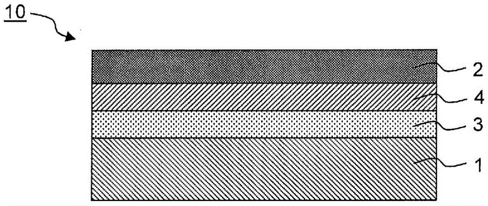
[0116] A thermosetting resin composition containing a melamine resin: an alkyd resin: an organosilane condensate at a weight ratio of 2:2:1 in terms of solid content was diluted with methyl ethyl ketone so that the solid content concentration was 8% by weight. The obtained diluted composition was coated on one main surface of a polymer film substrate made of a 50 μm thick PET film (manufactured by Mitsubishi Plastics, trade name “DIAFOIL”), and cured by heating at 150° C. for 2 minutes to form a film with a thickness of 35 nm. organic undercoating. The surface roughness of the formed organic undercoat layer was measured by AFM (manufactured by Seiko Instruments, "SPI3800"), and Ra was 0.5 nm.
[0117] (Formation of transparent conductive layer)
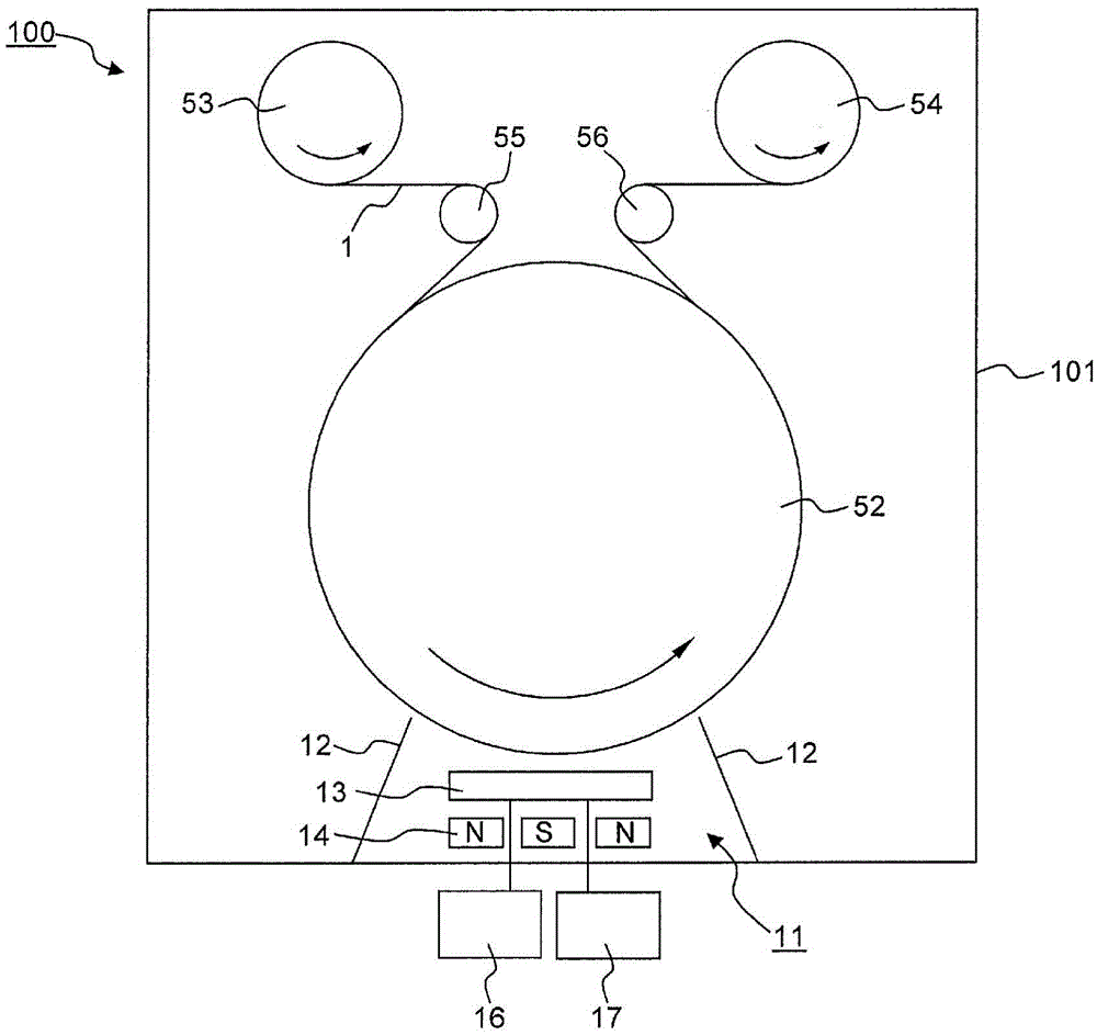
[0118] The polymer film base material that will be formed with above-mentioned organic undercoat is arranged in vacuum sputtering device, so that ultimate vacuum degree is 0.9 * 10 -4 The Pa ...
Embodiment 2
[0120] A transparent conductive layer and a transparent conductive film were produced in the same manner as in Example 1, except that a sintered body of 10% by weight tin oxide and 90% by weight indium oxide was used as a target to form a single-layer transparent conductive layer with a thickness of 25 nm.
Embodiment 3
[0122] In addition to setting the ultimate vacuum degree in the degassing process of the membrane to 2.0×10 -4 Except Pa, it carried out similarly to Example 2, and produced the transparent conductive layer and transparent conductive film.
PUM
| Property | Measurement | Unit |
|---|---|---|
| electrical resistivity | aaaaa | aaaaa |
| electrical resistivity | aaaaa | aaaaa |
| roughness | aaaaa | aaaaa |
Abstract
Description
Claims
Application Information
 - R&D Engineer
- R&D Manager
- IP Professional
- Industry Leading Data Capabilities
- Powerful AI technology
- Patent DNA Extraction
Browse by: Latest US Patents, China's latest patents, Technical Efficacy Thesaurus, Application Domain, Technology Topic, Popular Technical Reports.
© 2024 PatSnap. All rights reserved.Legal|Privacy policy|Modern Slavery Act Transparency Statement|Sitemap|About US| Contact US: help@patsnap.com


