Silicon substrate deep ultraviolet light emitting diode epitaxial chip structure and preparation method therefor
A technology of light-emitting diodes and epitaxial structures, applied in electrical components, circuits, semiconductor devices, etc., can solve the problems of low luminous efficiency of AlGaN deep-ultraviolet LEDs
- Summary
- Abstract
- Description
- Claims
- Application Information
AI Technical Summary
Problems solved by technology
Method used
Image

Examples
example 1
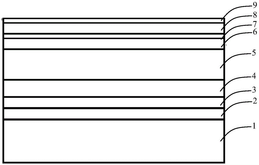
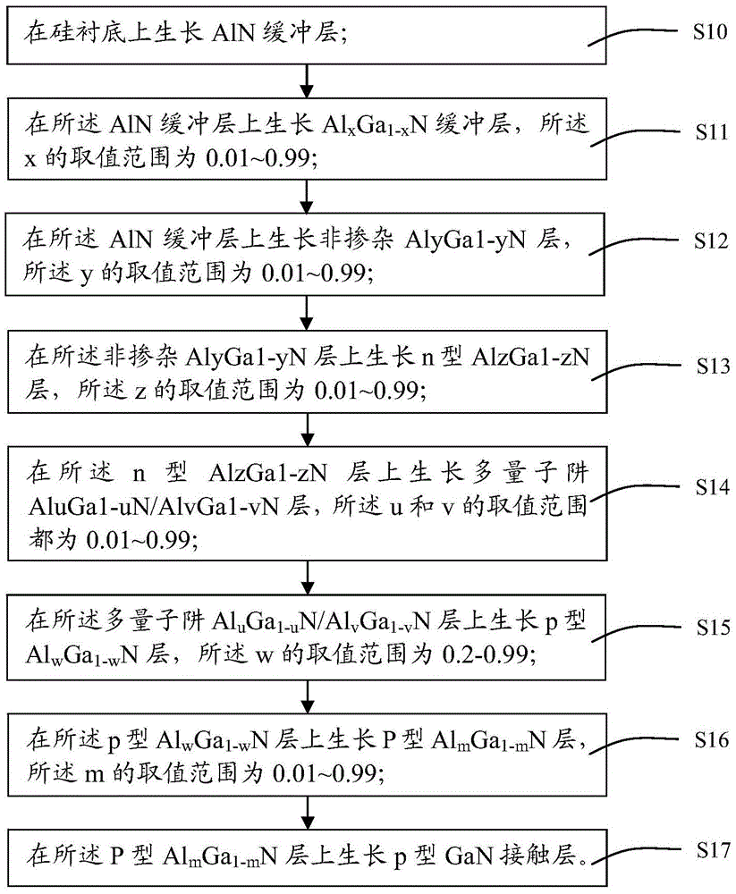
[0070] (1) if figure 1 As shown, select silicon substrate 1, after treatment, in MOCVD (metal organic compound chemical vapor deposition), with NH 3 and TMAl (trimethylaluminum) as raw materials, and grow an AlN buffer layer 2 with a thickness of 200 nm under the condition of 1200° C.
[0071] (2) In MOCVD, on the AlN buffer layer 2, with NH 3 , TMAl, TMGa (trimethylgallium) as raw materials, and grow Al with a thickness of 200nm at 1200°C 0.5 Ga 0.5 N buffer layer 3.
[0072] (3) In MOCVD, in Al 0.5 Ga 0.5 N buffer layer 3, with NH 3 , TMAl, and TMGa as raw materials, and grow non-doped Al with a thickness of 0.5um at 1400°C 0.5 Ga 0.5 N layer 4.
[0073] (4) In MOCVD, in non-doped Al 0.5 Ga 0.5 N layer 4, to NH 3 , TMAl, TMGa, SiH 4 as raw material (SiH 4 The doping concentration is 5E18cm -3 ), growing n-type Al with a thickness of 3um at 1400°C 0.5 Ga 0.5 N layer 5.
[0074] (5) In MOCVD, in n-type Al 0.5 Ga 0.5 N layer 5, to NH 3 , TMAl, and TMGa as r...
Embodiment 2
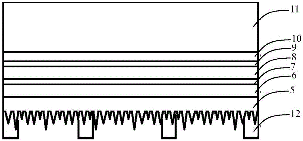
[0079] Based on the silicon substrate deep ultraviolet light emitting diode epitaxial structure provided in Example 1, in this embodiment, a silicon substrate deep ultraviolet light emitting diode chip structure is prepared, the structure is as follows figure 2 As shown, the following steps are included in the process of preparation:
[0080] After steps (1)~(8) in embodiment one, also include:
[0081] (9) Anneal the grown epitaxial structure, the annealing condition is: at 600°C, N 2 Annealed in the environment for 20min (minutes).
[0082] (10) After the annealing is completed, a layer of Al reflective electrode 10 with a thickness of 200 nm is sputtered on the surface of the p-type GaN contact layer 9 by sputtering.
[0083] (11) On the reflective electrode 10, the conductive silicon substrate 11 is bonded.
[0084] (12) The silicon substrate 1 is removed with KOH etching solution.
[0085] (13) AlN buffer layer 2, Al 0.5 Ga 0.5 N buffer layer 3 and non-doped Al 0....
example 3
[0089] (1) if figure 1 As shown, choose silicon substrate 1, after treatment, in MOCVD, with NH 3 and TMAl as raw materials, and grow an AlN buffer layer 2 with a thickness of 400 nm under the condition of 1200° C.
[0090] (2) In MOCVD, on the AlN buffer layer 2, with NH 3 , TMAl, and TMGa as raw materials, and grow Al with a thickness of 400nm at 1200°C 0.5 Ga 0.5 N buffer layer 3.
[0091] (3) In MOCVD, in Al 0.5 Ga 0.5 N buffer layer 3, with NH 3 , TMAl, and TMGa as raw materials, and grow non-doped Al with a thickness of 1.5um at 1400°C 0.3 Ga 0.7 N layer 4.
[0092] (4) In MOCVD, in non-doped Al 0.3 Ga 0.7 N layer 4, to NH 3 , TMAl, TMGa, SiH 4 as raw material (SiH 4 The doping concentration is 5E18cm -3 ), growing n-type Al with a thickness of 3um at 1400°C 0.3 Ga 0.7 N layer 5.
[0093] (5) In MOCVD, in n-type Al 0.3 Ga 0.7 N layer 5, to NH 3 , TMAl, and TMGa as raw materials, and grow Al at 1400°C 0.2 Ga 0.8 N / Al 0.4 Ga 0.6 N periodic structur...
PUM
| Property | Measurement | Unit |
|---|---|---|
| Thickness | aaaaa | aaaaa |
| Thickness | aaaaa | aaaaa |
| Growth temperature | aaaaa | aaaaa |
Abstract
Description
Claims
Application Information
 - R&D
- Intellectual Property
- Life Sciences
- Materials
- Tech Scout
- Unparalleled Data Quality
- Higher Quality Content
- 60% Fewer Hallucinations
Browse by: Latest US Patents, China's latest patents, Technical Efficacy Thesaurus, Application Domain, Technology Topic, Popular Technical Reports.
© 2025 PatSnap. All rights reserved.Legal|Privacy policy|Modern Slavery Act Transparency Statement|Sitemap|About US| Contact US: help@patsnap.com