Ceramic substrate circuit board and manufacturing method thereof
A technology of ceramic substrate and manufacturing method, which is applied in the direction of printed circuit manufacturing, printed circuit, circuit substrate materials, etc., can solve problems affecting the processing technology of ceramic substrates, affecting the overall performance of ceramic substrate circuit boards, uneven or skewed aluminum sheets, etc. Achieve the effects of prolonging service life, reducing thickness, improving oxidation resistance and wear resistance
- Summary
- Abstract
- Description
- Claims
- Application Information
AI Technical Summary
Problems solved by technology
Method used
Image

Examples
Embodiment 1
[0015] This embodiment provides a ceramic substrate circuit board, including a ceramic substrate, a palladium-silver pad embedded on the ceramic substrate through a sintering process, and an anti-oxidation layer, and the anti-oxidation layer is attached to the palladium-silver pad through an electroplating process away from the outer surface of the ceramic substrate. Those skilled in the art can understand that the anti-oxidation layer is attached to the palladium-silver pad through the electroplating process, and the structure of the anti-oxidation layer is more smooth and stable, which can effectively improve the overall performance of the ceramic substrate circuit board. In addition, compared with the soldering technology in the prior art, since the solder layer is omitted between the anti-oxidation layer and the palladium-silver pad, the thickness of the ceramic substrate circuit board can be effectively reduced, and the electronic circuit board manufactured by using the ci...
Embodiment 2
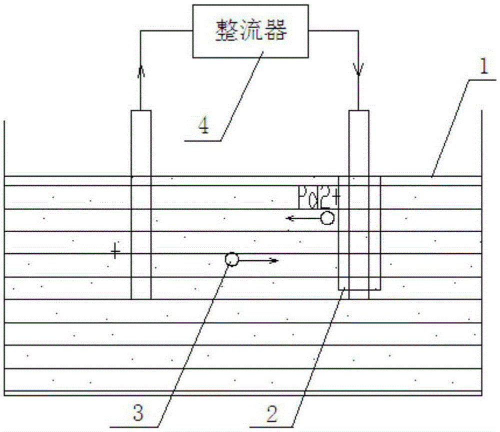
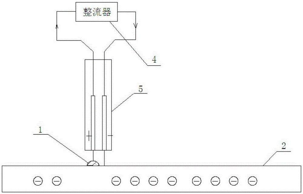
[0018] Such as figure 1 As shown, the present embodiment provides a method for manufacturing a ceramic substrate circuit board 2, comprising the following steps:
[0019] Step 1, embedding the palladium-silver paste on the ceramic substrate through a sintering process to form a palladium-silver pad;
[0020] Step 2. Attach the anti-oxidation material to the surface of the palladium-silver pad far away from the ceramic substrate through an electroplating process to form an anti-oxidation layer.
[0021] Those skilled in the art can understand that the anti-oxidation layer is attached to the palladium-silver pad through the electroplating process, and the structure of the anti-oxidation layer is more smooth and stable, which can effectively improve the overall performance of the ceramic substrate circuit board 2 . In addition, compared with the solder soldering technology in the prior art, since the solder layer is omitted between the anti-oxidation layer and the palladium-silv...
Embodiment 3
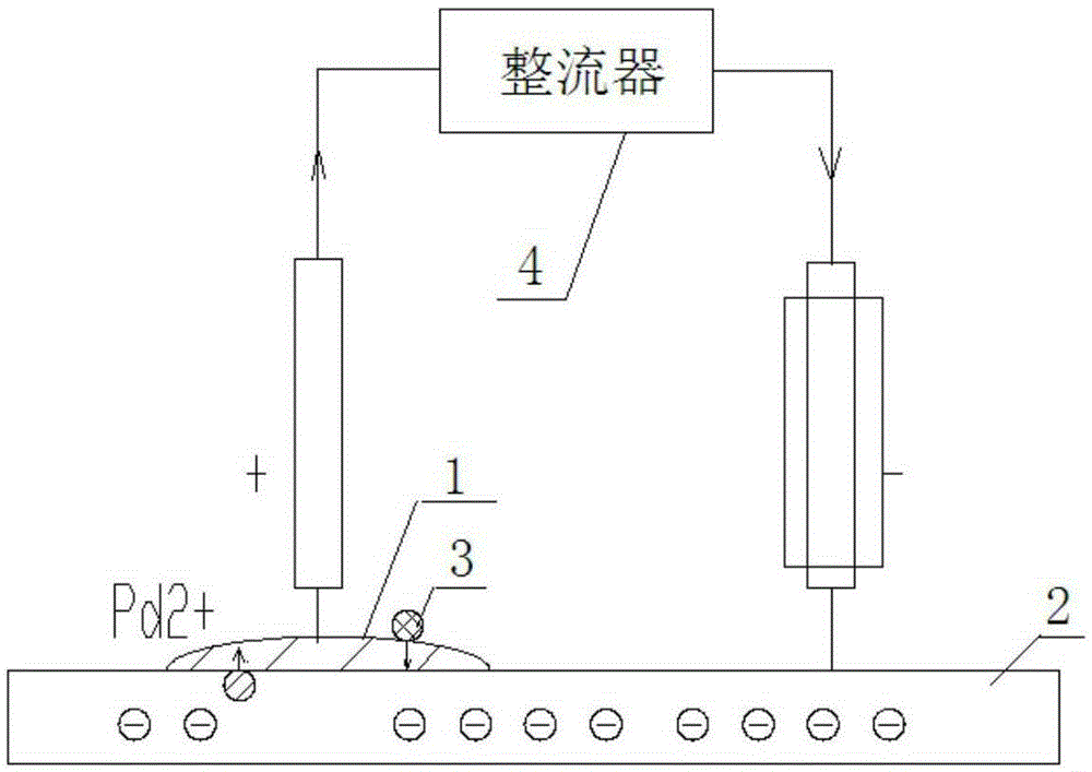
[0029] Such as figure 2 As shown, the present embodiment provides a method for manufacturing a ceramic substrate circuit board 2, comprising the following steps:
[0030] Step 1, embedding the palladium-silver paste on the ceramic substrate through a sintering process to form a palladium-silver pad;
[0031] Step 2. Attach the anti-oxidation material to the surface of the palladium-silver pad far away from the ceramic substrate through an electroplating process to form an anti-oxidation layer.
[0032] Those skilled in the art can understand that the anti-oxidation layer is attached to the palladium-silver pad through the electroplating process, and the structure of the anti-oxidation layer is more smooth and stable, which can effectively improve the overall performance of the ceramic substrate circuit board 2 . In addition, compared with the solder soldering technology in the prior art, since the solder layer is omitted between the anti-oxidation layer and the palladium-sil...
PUM
 Abstract
Description
Claims
Application Information
 - R&D
- Intellectual Property
- Life Sciences
- Materials
- Tech Scout
- Unparalleled Data Quality
- Higher Quality Content
- 60% Fewer Hallucinations
Browse by: Latest US Patents, China's latest patents, Technical Efficacy Thesaurus, Application Domain, Technology Topic, Popular Technical Reports.
© 2025 PatSnap. All rights reserved.Legal|Privacy policy|Modern Slavery Act Transparency Statement|Sitemap|About US| Contact US: help@patsnap.com