Preparation method for flexible mask plate used for patterning curved surface
A technology of patterning and masking, which is applied in the manufacturing field of curved surface occlusion patterning, can solve problems such as difficulty in execution, and achieve the effect of avoiding cumbersome process steps.
- Summary
- Abstract
- Description
- Claims
- Application Information
AI Technical Summary
Problems solved by technology
Method used
Image
Examples
Embodiment 1
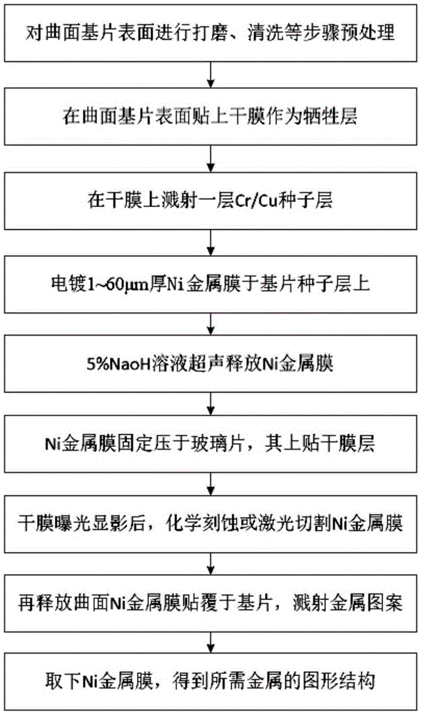
[0035] The metal Ni film is etched for depositing a layer of thermistor wire sensor structure on the insulating curved surface.
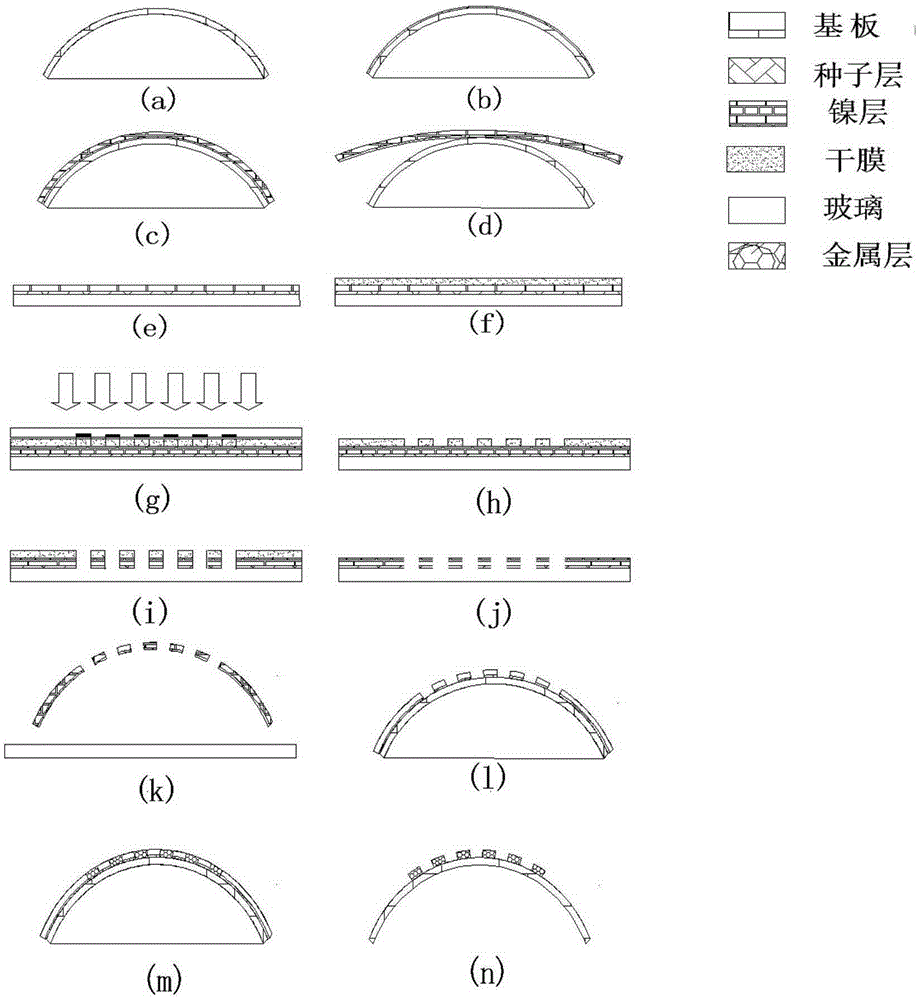
[0036] The first step is to carry out the film sticking process on the convex and concave sides of the curved surface. Make sure the blades are cleaned before applying the film, and pay attention to avoid air bubbles when applying the film. After the film is pasted, put it into the oven and bake at 90°C for 30 minutes.
[0037] In the second step, fix the curved surface with polyimide tape, place it well, and perform sputtering to sputter the Cr / Cu seed layer. The thickness of the Cr metal layer is 1-100 nm, and the thickness of the Cu metal layer is 1-200 nm.
[0038] The third step is electroplating a Ni metal layer on the curved substrate seed layer. Dots of photoresist on the curved surface are used to create release holes. Electroplating needs to be carried out in a water bath at 50°C, the workpiece is connected to the negative electrode, a...
Embodiment 2
[0046] Laser-cut metal Ni film patterns are used for occlusion curved surface masks, and a layer of thermistor wire sensor structure is deposited on the insulating curved surface.
[0047] The first step is to carry out the film sticking process on the convex and concave sides of the curved surface. Make sure the blades are cleaned before applying the film, and pay attention to avoid air bubbles when applying the film. After the film is pasted, put it into the oven and bake at 90°C for 30 minutes.
[0048] In the second step, the curved surface is fixed with polyimide tape, placed, and sputtered. A Cr / Cu seed layer was sputtered. The thickness of the Cr metal layer is 1-100 nm, and the thickness of the Cu metal layer is 1-200 nm.
[0049] The third step is electroplating a Ni metal layer on the curved substrate seed layer. Dots of photoresist on the curved surface are used to create release holes. Electroplating needs to be carried out in a water bath at 50°C, the workpie...
PUM
| Property | Measurement | Unit |
|---|---|---|
| thickness | aaaaa | aaaaa |
| thickness | aaaaa | aaaaa |
| thickness | aaaaa | aaaaa |
Abstract
Description
Claims
Application Information
 - R&D
- Intellectual Property
- Life Sciences
- Materials
- Tech Scout
- Unparalleled Data Quality
- Higher Quality Content
- 60% Fewer Hallucinations
Browse by: Latest US Patents, China's latest patents, Technical Efficacy Thesaurus, Application Domain, Technology Topic, Popular Technical Reports.
© 2025 PatSnap. All rights reserved.Legal|Privacy policy|Modern Slavery Act Transparency Statement|Sitemap|About US| Contact US: help@patsnap.com


