Manufacture method for plugging resin into soft and hard combined circuit board

A soft-rigid combination, resin plug hole technology, applied in multilayer circuit manufacturing, printed circuit manufacturing, printed circuit and other directions, can solve the problems of labor and time, difficult groove 29, difficult to remove resin 28, etc., to reduce rework , Guarantee the effect of drilling position thickness

Inactive Publication Date: 2016-01-06
SHENZHEN SUNTAK MULTILAYER PCB
View PDF6 Cites 5 Cited by
  • Summary
  • Abstract
  • Description
  • Claims
  • Application Information

AI Technical Summary

Problems solved by technology

[0005] like figure 2 As shown, when making the inner layer pattern, the solder pad corresponding to the via hole 26 of the inner layer copper layer 24 is etched away, and the NO-FLOWPP glue used for the lamination of the soft and hard combined circuit board has poor fluidity, and the via hole 26 after pressing The copper-free position of the corresponding inner layer copper layer 24 is filled by the adjacent first base material 21 and the second base material 22, thereby causing the surface of the corresponding position of the first base copper 23 on the surface of the first base material 21 and the second base copper on the surface of the second base material 22. The corresponding position of the dibase copper 25 is depressed; after drilling, the graphic plated hole will be plated with a certain thickness of copper on the surface near the via hole 26, and the copper plating 27 on the surface forms an annular groove 29 with the depression on the surface, and The groove 29 is difficult to be polished and smooth. After the resin 28 plugs the hole, the resin 28 overflowing into the groove 29 is difficult to remove through the abrasive belt grinding plate, and manual grinding is required, which consumes a lot of labor and time.

Method used


Image

  • Manufacture method for plugging resin into soft and hard combined circuit board
  • Manufacture method for plugging resin into soft and hard combined circuit board

Examples


Embodiment 1

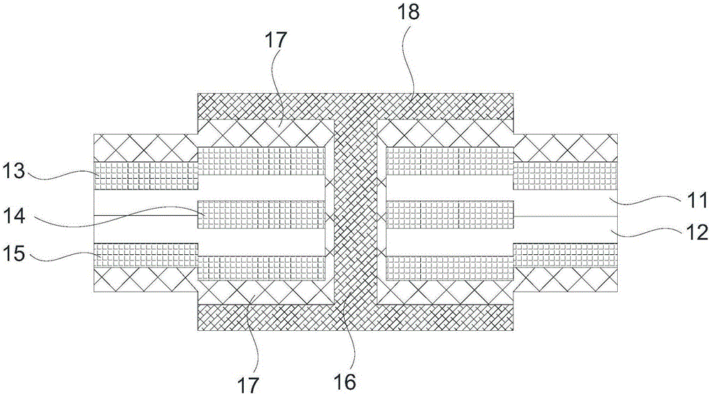
[0031] Such as figure 1 The shown three-layer flex-rigid circuit board includes a first base material 11, a second base material 12, an inner layer of wiring copper between the first base material 11 and the second base material 12, and the surface of the first base material 11 is covered with There is a first base copper 13 , and the surface of the second base material 12 is covered with a first base copper 15 . Resin plug holes 16 that can be used to make pads on the surface need to be made on the flexible and rigid circuit board. The manufacturing method includes the following steps:

[0032] Make the inner circuit pattern, and the drill hole corresponding to the circuit pattern leaves an isolated pad 14 larger than the diameter of the resin plug hole 16; the diameter of the isolated pad is 0.35mm larger than the diameter of the resin plug hole 16.

[0033] Use NO-FLOWPP to press to form a rigid-flex circuit board. After lamination, the surface of the rigid-flex circuit b...

Embodiment 2

[0041] The PCB with the following parameter requirements is manufactured by using the manufacturing method of the resin plug hole of the present invention.

[0042] Inner core board:

[0043] 0.075mm0.5 / 0.5OZ (without copper) (2 pieces);

[0044] Number of layers: 8 layers;

[0045] Inner line width / line spacing: 0.1mm / 0.1mm, 0.091mm / 0.1mm

[0046] Outer layer line width / line spacing: 0.1 / 0.1mm (finished copper thickness 1.0OZ);

[0047] Sheet Tg: ≥170°;

[0048] Outer core board 0.36mm0.5 / 0.5oz (without copper) (2 pieces): 1 / 2OZ;

[0049] Hole copper thickness: 18um(min) / 20um(ave);

[0050] Surface treatment: immersion gold;

[0051] Finished board thickness: 1.6mm±10%;

[0052] Minimum drill bit: 0.2mm;

[0053] Drilling thickness to diameter ratio: 8:1;

[0054] Production PNL size: 304mm×457mm.

[0055] The specific production process is as follows:

[0056] 1. Cutting - According to the number of core boards with different thicknesses required and the PNL size ...


PUM

PropertyMeasurementUnit
Thicknessaaaaaaaaaa
Thicknessaaaaaaaaaa
Thicknessaaaaaaaaaa

Abstract

The invention discloses a manufacture method for plugging resin into a soft and hard combined circuit board, and relates to the technical field of circuit board production. The method comprises that S1) an internal circuit pattern is prepared in both a soft core board and a hard core board, and corresponding drilling positions of the circuit pattern are provided with isolated pads whose aperture is greater than that of a drill hole; S2) the soft core board and the hard core board are compressed by PP to form the soft and hard combined circuit board; S3) the drill hole into which resin needs to be plugged is drilled in the soft and hard combined circuit board; S4) copper deposition and electroplating are carried out on the inner wall of the drill hole; S5) the electroplated drill hole is filled with the resin, and the resin is solidified initially; and S6) and residual resin flowing out of the copper surface of the soft and hard combined circuit board is polished by a polishing plate. The isolated pads of the internal circuit in the drilling pole positions are reserved, the thickness of the drilling hole positions is ensured, the problem that the copper surface at the through hole position is recessed caused by low filling capability of NO-FLOW PP used in the soft and hard combined circuit board is solved, and rework of manual polishing due to the fact that the resin polishing plate is not clean is reduced.

Description

technical field [0001] The invention relates to the technical field of circuit board production, in particular to a method for manufacturing a resin plug hole of a soft-hard combination circuit board. Background technique [0002] In the design of flexible and rigid circuit boards, due to the limitation of product design and wiring space, vias are provided under some surface pads. In order to ensure the soldering quality of components on the surface pads, the vias under the surface pads need to be applied to plugs Hole process to ensure the flatness of the surface pad. [0003] Resin ink plugging is the most commonly used plugging process at present. After making the inner layer graphics, pressing, drilling, and graphic plating, the via holes are filled with resin ink by screen or aluminum sheet printing, and after baking and curing, the abrasive belt grinder grinds off the resin overflowing the copper surface and removes it. Level the surface of the plate, and then sink t...

Claims


Application Information

Patent Timeline
IPC IPC(8): H05K3/46
CPCH05K3/4608H05K3/4691H05K2201/0959
Inventor 宇超王淑怡何淼
Owner SHENZHEN SUNTAK MULTILAYER PCB
Why Eureka
Try Eureka