High Thermal Conductivity SMD Bypass Diodes

A bypass diode, high thermal conductivity technology, applied in the field of diodes, can solve the problems of increasing the volume and cost of the junction box, large forward voltage drop of the bypass diode, and poor heat dissipation effect of the junction box, so as to improve the heat dissipation effect and reduce the volume. , the effect of good thermal conductivity

Active Publication Date: 2017-11-28
CHANGZHOUSR SEA ELECTRONICS
View PDF6 Cites 4 Cited by
  • Summary
  • Abstract
  • Description
  • Claims
  • Application Information

AI Technical Summary

Problems solved by technology

Since the traditional package of the bypass diode in the junction box is R-6, this kind of package takes up a lot of space in the circuit, which increases the size and cost of the junction box, and the heat generated by the R-6 package diode is large, which reduces the The service life of the junction box is shortened, and the promised 20-25 years cannot be achieved. Moreover, the forward voltage drop of the bypass diode is too large, and the heat dissipation effect of the junction box is not good, which can easily cause thermal breakdown of the bypass diode and cause damage to the junction box. With the phenomenon of junction box burning, etc., it is urgent to improve the structure and production process of the existing bypass diodes

Method used


Image

  • High Thermal Conductivity SMD Bypass Diodes

Examples


Embodiment Construction

[0026] The present invention will be further described below in conjunction with the accompanying drawings.

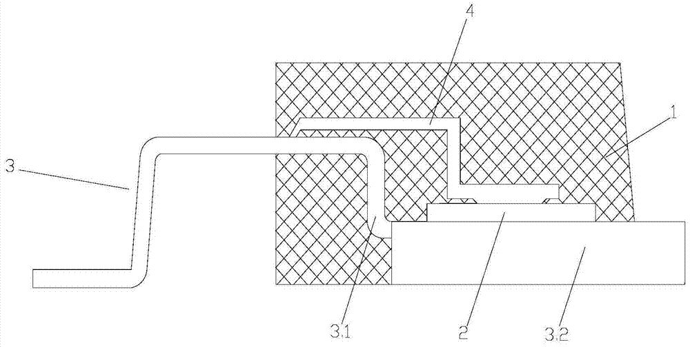
[0027] refer to figure 1 The high thermal conductivity chip bypass diode shown includes a body 1, a chip 2 made of deep-channel silicon technology, and a copper frame patch 3. The chip 2 and the frame patch 3 are molded in a half-package package structure In the body 1 of high thermal conductivity and low stress vinyl, the frame patch 3 is a stepped integrated structure composed of a thin piece 3.1 and a thick piece 3.2. The side of the thin piece 3.1 is higher than the side of the thick piece 3.2, and the connection between the thin piece 3.1 and the thick piece 3.2 Extend vertically upwards and then horizontally, and extend to the outside of the left side of the body 1. One end of the core particle 2 is soldered to the upper surface of the thick sheet 3.2 close to the step structure by soldering technology. Soldering can effectively control the welding porosity To i...


PUM


Abstract

The invention belongs to the technical field of diodes, and specifically relates to a bypass diode with a high thermal conductivity patch, including a body, a chip made by a deep channel silicon process, and a frame patch. In the body of heat-conducting low-stress vinyl, the frame patch is a stepped structure composed of a thin piece and a thick piece. One side of the thin piece is higher than the side of the thick piece, and one end of the core is soldered to the thick piece close to the step structure. On the surface, the other end of the chip is connected to the chip with a jumper wire. The bottom surface of the thick chip is flush with the bottom surface of the body. The end of the thick chip extends out of one side of the body to form a lead structure. The end of the chip extends horizontally from the other side of the body and bends downward. Then it is extended horizontally to form a lead structure. The bottom of the lead mechanism formed at the end of the sheet is flush with the bottom of the thick sheet. The welding area is large and has better heat dissipation performance. At the same time, the forward voltage drop is significantly reduced and the power consumption is reduced. And heat, greatly improving the service life.

Description

technical field [0001] The invention belongs to the technical field of diodes, in particular to a patch bypass diode with high thermal conductivity. Background technique [0002] Solar photovoltaic cell is a photoelectric conversion device made of semiconductor photovoltaic effect, which can be used as both a power source and a photoelectric detection device. Solar cell modules are often installed outdoors or in relatively open places far away from the city. When one or several cells in the solar cell module are blocked by other objects for a long time, the blocked solar cells will be seriously heated or even burned out. This is the "hot spot effect". This effect can cause serious damage to solar cells. Some or all of the energy generated by the illuminated cell may be dissipated by the shaded cell. In order to prevent the solar cells from being damaged due to the thermal shift effect, a photovoltaic bypass diode needs to be connected in parallel between the positive and ...

Claims


Application Information

Patent Timeline
Patent Type & Authority Patents(China)
IPC IPC(8): H02S40/34
CPCH01L2924/181H01L2224/40245Y02E10/50H01L2924/00012
Inventor 何永成赵帅帅
Owner CHANGZHOUSR SEA ELECTRONICS
Why Eureka
Try Eureka