An LED epitaxial layer growth method and an epitaxial layer structure and an LED chip obtained through the method
A technology of LED chip and growth method, applied in the direction of electrical components, circuits, semiconductor devices, etc., can solve the problem of low reverse voltage, and achieve the effect of improving reverse voltage, good transition, and reducing differences
- Summary
- Abstract
- Description
- Claims
- Application Information
AI Technical Summary
Problems solved by technology
Method used
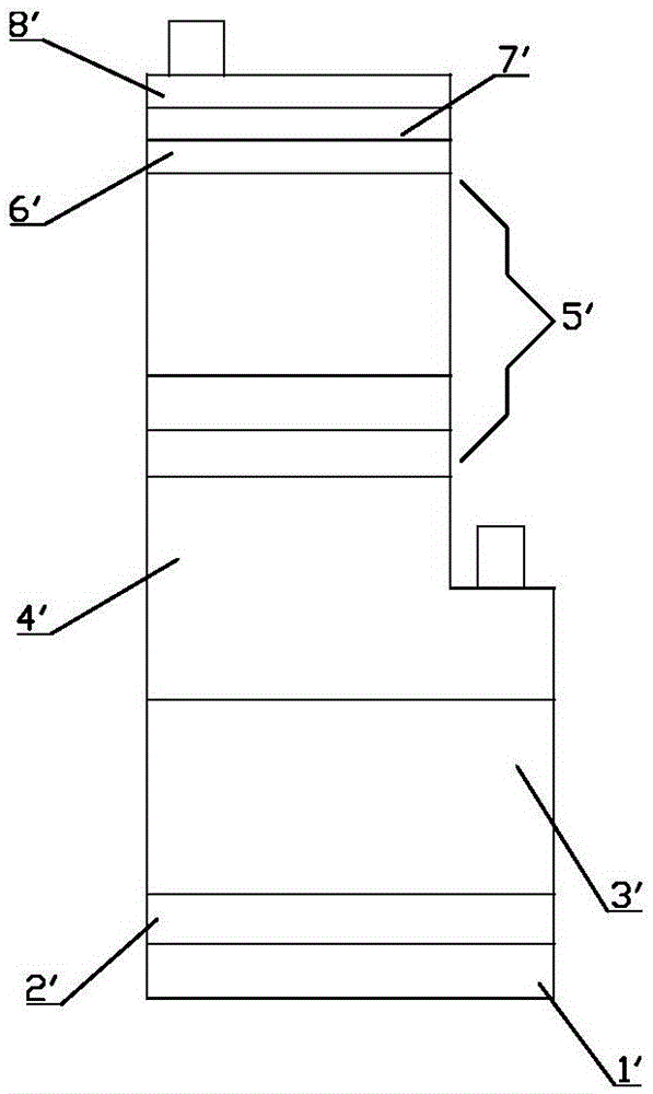
Image


Examples
Embodiment 1
[0044] 1. Process the sapphire substrate for about 6 minutes at 1000°C and maintain the reaction chamber pressure at 150mbar in a hydrogen atmosphere;
[0045] 2. Cool down to 550°C, maintain the pressure in the reaction chamber at 550mbar, and feed NH 3 , TMGa grows a low-temperature buffer layer GaN with a thickness of 30nm on the sapphire substrate;
[0046] 3. Raise the temperature to 1100°C, maintain the pressure in the reaction chamber at 300mbar, and feed NH 3 , TMGa, continuous growth of 2-4μm undoped GaN;
[0047] 4. Then pass into NH 3 , TMGa, SiH 4 Continuous growth of Si-doped N-type GaN, Si doping concentration 9E+18atom / cm 3 , the total thickness is controlled at 2 μm;
[0048] 5. Periodically grow the luminescent layer MQW, the pressure of the reaction chamber is maintained at 300mbar, and NH is fed at a low temperature of 700°C 3 , TEGa, TMIn growth doped In thickness of 2.5nmIn x Ga (1-x) N(x=0.15) layer, heat up to 800°C and feed NH 3 , TEGa grows a ...
Embodiment 2
[0054] 1. Process the sapphire substrate for about 6 minutes at 1100°C and maintain the reaction chamber pressure at 200mbar in a hydrogen atmosphere;
[0055] 2. Cool down to 600°C, maintain the pressure in the reaction chamber at 600mbar, and feed NH 3 , TMGa grows a low-temperature buffer layer GaN with a thickness of 40nm on a sapphire substrate;
[0056] 3. Raise the temperature to 1100°C, maintain the pressure in the reaction chamber at 300mbar, feed NH3 and TMGa, and continue to grow 2μm undoped GaN;
[0057] 4. Then pass into NH3, TMGa, SiH 4 Continuous growth of N-type GaN doped with Si, Si doping concentration 2E+19atom / cm 3 , the total thickness is controlled at 4 μm;
[0058]5. Periodically grow the light-emitting layer MQW, the pressure of the reaction chamber is maintained at 350mbar, and the thickness of doped In is 3nmIn by feeding NH, TEGa, and TMIn at a low temperature of 750°C. x Ga (1-x) N(x=0.25) layer, heat up to 850°C and feed NH 3 , TEGa grows a G...
Embodiment 3
[0064] 1. Process the sapphire substrate for about 6 minutes at 1050°C and maintain the reaction chamber pressure at 150mbar in a hydrogen atmosphere;
[0065] 2. Cool down to 550°C, maintain the pressure in the reaction chamber at 550mbar, and feed NH 3 , TMGa grows a low-temperature buffer layer GaN with a thickness of 36nm on a sapphire substrate;
[0066] 3. Raise the temperature to 1120°C, maintain the pressure in the reaction chamber at 300mbar, and feed NH 3 , TMGa, continuous growth of 3μm undoped GaN;
[0067] 4. Then pass into NH 3 , TMGa, SiH 4 Continuous growth of Si-doped N-type GaN, Si doping concentration 1E+19atom / cm 3 , the total thickness is controlled at 3 μm;
[0068] 5. The luminescent layer MQW is grown periodically, the pressure of the reaction chamber is maintained at 300mbar, and NH is fed at a low temperature of 740°C 3 , TEGa, TMIn growth doped In thickness of 2.7nmIn x Ga (1-x) N(x=0.2) layer, heat up to 840°C and feed NH 3 , TEGa grows a G...
PUM
 Abstract
Description
Claims
Application Information
 - R&D
- Intellectual Property
- Life Sciences
- Materials
- Tech Scout
- Unparalleled Data Quality
- Higher Quality Content
- 60% Fewer Hallucinations
Browse by: Latest US Patents, China's latest patents, Technical Efficacy Thesaurus, Application Domain, Technology Topic, Popular Technical Reports.
© 2025 PatSnap. All rights reserved.Legal|Privacy policy|Modern Slavery Act Transparency Statement|Sitemap|About US| Contact US: help@patsnap.com