
Aromatic heterocyclic compound, manufacturing method thereof, organic semiconductor material, and organic semiconductor device

An aromatic heterocyclic and organic semiconductor technology, applied in semiconductor devices, semiconductor/solid-state device manufacturing, electrical components, etc., to achieve the effects of good film formation, high technical value, and high solubility

Active Publication Date: 2015-11-18
NIPPON STEEL CHEM &MATERIAL CO LTD
View PDF8 Cites 7 Cited by
  • Summary
  • Abstract
  • Description
  • Claims
  • Application Information

AI Technical Summary

Problems solved by technology

[0011] For example, although it has been proposed that a polycyclic ring-condensed compound having two benzofuran skeletons, indole skeletons or benzothiophene skeletons condensed on a naphthalene ring is used as an organic thin film transistor ( thinfilmtransistor, TFT) organic semiconductor layer material, but there are no specific examples of introducing two or more heteroatoms (Patent Document 2, Patent Document 3)

Method used

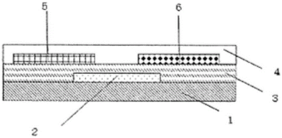
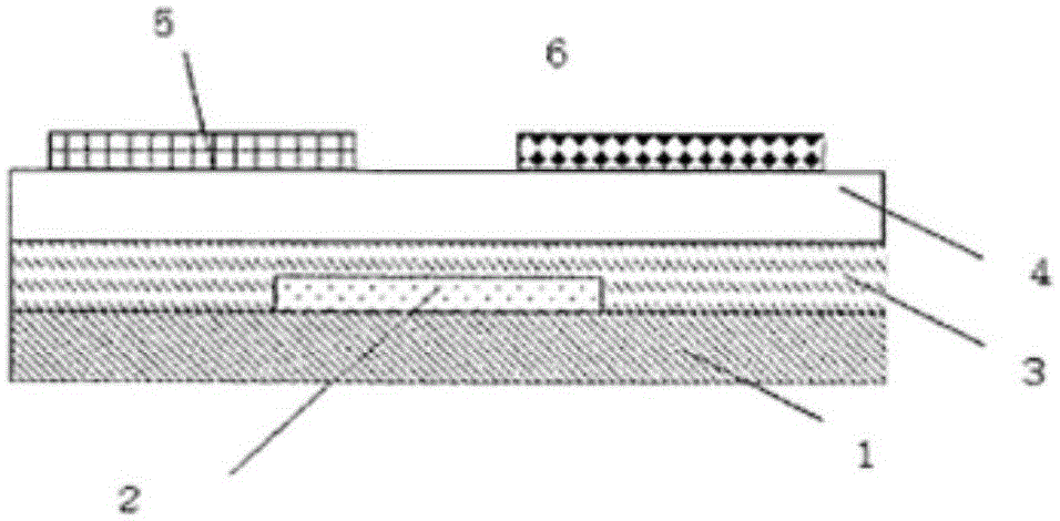
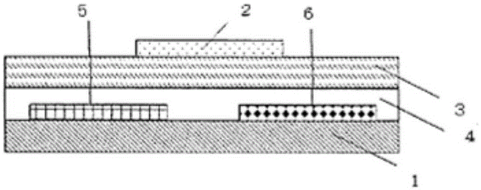

Image

  • Aromatic heterocyclic compound, manufacturing method thereof, organic semiconductor material, and organic semiconductor device
  • Aromatic heterocyclic compound, manufacturing method thereof, organic semiconductor material, and organic semiconductor device
  • Aromatic heterocyclic compound, manufacturing method thereof, organic semiconductor material, and organic semiconductor device

Examples


Embodiment 1

[0199] [chem 37]

[0200]

[0201] Under nitrogen flow, dibenzothiophene (1-A) (109 mmol, 20.0 g) and dehydrated tetrahydrofuran (THF) (100 mL) were added to a 1000 mL reactor, and stirred at 0° C. for 30 minutes. 2N BuLi-hexane solution (60 mL, 156 mmol) was added dropwise thereto. After the dropwise addition was completed, the mixture was heated to reflux for 6 hours. After cooling to room temperature, dehydrated dimethylformamide (dimethylformamide, DMF) (20 mL, 160 mmol) was added dropwise, followed by stirring overnight at room temperature. The reaction mixture was poured into 6N hydrochloric acid (500 mL), extracted with acetic acid, and the organic layer was washed with water and dried. Compound (1-B) 8.0 g was obtained by column chromatography.

[0202] Under nitrogen flow, 3-bromopropionic acid (1-C) (169 mmol, 25 g) and triphenylphosphine (196 mmol, 51.42 g), dehydrated acetonitrile (70 mL) were added to a 500 mL reactor. After the addition, the mixture was st...

Embodiment 2

[0211] [chem 39]

[0212]

[0213] Under a nitrogen atmosphere, compound (101) (7.7mmol, 2.5g), DMF (120mL), 62% NaH (8.4mmol, 0.34g), iodoctane (8.4mmol, 2.1g) were added to a 200mL three-necked flask ), and stirred overnight at room temperature. A small amount of methanol was added to the reaction solution, and after confirming no bubbling, the reaction mixture was poured into water, and the precipitate was separated by filtration and washed with methanol and hexane to obtain 2.4 g of the target compound (201). The NMR spectrum data of the obtained compound (compound A201) is shown in Figure 9 middle.

Embodiment 3

[0215] [chemical 40]

[0216]

[0217] Under a nitrogen stream, dibenzofuran (2-A) (3448 mmol, 580 g) and dehydrated THF (2260 mL) were added to a 10 L reactor, and stirred at 0° C. for 30 minutes. Thereto, a 1.6M BuLi-heptane solution (3414 mmol, 2134 mL) was added dropwise. After stirring at -78°C for 30 minutes, DMF (5173 mmol, 401 mL) was added dropwise. After it was warmed to room temperature, stirring was continued for 2 hours. The reaction solution was poured into 6M hydrochloric acid, and the pH value was adjusted to 1. This was extracted with ethyl acetate, washed with water and brine, dried over sodium sulfate, filtered, and concentrated to obtain 690 g of a crude compound (2-B) as a yellow-white solid.

[0218] Under nitrogen flow, add compound (2-B) (3411mmol, 690g) and Wittig salt (1-D) (3377mmol, 1402g), dehydrated THF (6L), dehydrated DMSO (6L) in the reactor of 20L , stirred at 27°C (water bath) for 30 minutes. Sodium hydride (7164mmol, 286g) was inject...


PUM


Abstract

Provided are an organic semiconductor material having high charge transfer capability, oxidation stability, and solvent solubility, as well as an organic semiconductor element using this material, a new aromatic heterocyclic compound used in this element, and a method of manufacturing the compound. The aromatic heterocyclic compound is expressed by general formula (1), the compound having two hetero atoms, and having a structure that condenses six rings. In the formula, X represents an oxygen atom or N-R, and R represents a hydrogen atom or a monovalent substitution group. The organic semiconductor material contains this aromatic heterocyclic compound, and is used in organic devices such as organic semiconductor films, organic thin-film transistors, and organic photovoltaic elements.

Description

technical field [0001] The present invention relates to a novel aromatic heterocyclic compound, an organic semiconductor material containing the same, an organic semiconductor film obtained by using the organic semiconductor material, and an organic semiconductor element such as an organic field effect transistor. Background technique [0002] In general, a semiconductor element using silicon, an inorganic semiconductor material, requires a high-temperature process and a high-vacuum process to form a thin film. Since a high-temperature process is required, it is impossible to form a thin film of silicon on a plastic substrate or the like, so it is difficult to impart flexibility or reduce weight to a product incorporating a semiconductor element. In addition, since a high-vacuum process is required, it is difficult to increase the size and cost of products incorporating semiconductor elements. [0003] Therefore, in recent years, organic semiconductor elements using organic...

Claims


Application Information

Patent Timeline
Patent Type & Authority Applications(China)
IPC IPC(8): C07D495/04H01L29/786H01L51/05H01L51/30C07D491/048
CPCC07D495/04C07D491/048H01L51/0071H01L51/0558H10K85/657H10K10/484H10K30/50Y02E10/549Y02P70/50H10K85/655H10K85/6574H10K85/40H10K30/00
Inventor 川田敦志长浜拓男林田広幸桝谷浩太
Owner NIPPON STEEL CHEM &MATERIAL CO LTD
Learn More