PCB bonding pad/line connection structure

A PCB circuit board and circuit connection technology, applied in the direction of electrical connection of printed components, printed circuits, printed circuits, etc. Stable performance, ensuring the effect of finished product quality

Inactive Publication Date: 2015-10-21
竞陆电子(昆山)有限公司
View PDF4 Cites 5 Cited by
  • Summary
  • Abstract
  • Description
  • Claims
  • Application Information

AI Technical Summary

Problems solved by technology

[0003] In the current CAM design, the length of one side of the solder mask window is usually designed to be 2.5mil, and the length of the tear drop is usually designed to be 3mil; Offset (1.5mil) and undercut due to ink corrosion (1mil), while the risk value of the Giavanni effect caused by solder mask ope...

Method used


Image

  • PCB bonding pad/line connection structure

Examples


Embodiment Construction

[0015] Preferred embodiments of the present invention will be described in detail below with reference to the drawings.

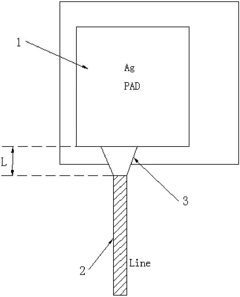
[0016] A pad / line connection structure of a PCB circuit board according to the present invention, the PCB circuit board includes a substrate, the substrate is provided with a connected pad 1 and a circuit 2; the connection between the pad and the circuit A teardrop structure 3 is also added, and the length of the teardrop structure satisfies the following formula:

[0017] L≥o+e+a

[0018] In the formula, L is the length of the added teardrop structure, o is the size of one side of the solder mask window, e is the offset of the solder mask, and a is the amount of side erosion of the ink.

[0019] This embodiment takes a PCB circuit board with a line spacing of less than 9mil as an example. In the above formula for calculating the length of the teardrop structure, the value of o is the maximum value on one side of the solder mask window, which is 1.5mil; th...


PUM


Abstract

The invention discloses a PCB bonding pad/line connection structure. A PCB comprises a substrate. The substrate is provided with a bonding pad and a line which are connected. The connection place of the bonding pad and the line is provided with a teardrop structure, and the length of the teardrop structure meets the following formula: L>=o+e+a, wherein the L is the length of the teardrop structure, the o is the dimension of a single edge of a solder mask window, the e is solder resist offset and the a is ink lateral erosion amount. By comprehensively considering the solder mask window information, the solder resist offset and the ink lateral erosion information, a teardrop in a suitable size is obtained, and the length of the teardrop added to the connection place between the bonding pad and the line is allowed to be larger than the risk value generated due to the galvanic effect, thereby preventing the phenomenon that the connection place between the bonding pad and the line is etched broken, ensuring quality of finished products of a PCB effectively and ensuring stability of electrical performance of the PCB.

Description

technical field [0001] The invention relates to the technical field of circuit boards, and specifically provides a pad / line connection structure of a PCB circuit board. Background technique [0002] The micro-etching carried out before the surface treatment of the PCB circuit board is easy to cause a micro-open circuit phenomenon at the connection between the pad and the line, which is the Giavani effect. Therefore, when the PCB circuit board is designed in CAM, it is usually necessary to add teardrops (Teardrop) at the connection between the pad and the circuit to ensure the electrical performance of the finished circuit. [0003] In the current CAM design, the length of one side of the solder mask window is usually designed to be 2.5mil, and the length of the teardrop is usually designed to be 3mil; Offset (1.5mil) and undercut due to ink corrosion (1mil), while the risk value of the Giavanni effect caused by solder mask opening, solder mask offset, and ink undercut is 5m...

Claims


Application Information

Patent Timeline
IPC IPC(8): H05K1/11
CPCH05K1/111H05K2201/09381H05K2201/09427
Inventor 李泽清
Owner 竞陆电子(昆山)有限公司
Why Eureka
Try Eureka