Built-in nanometer channel cooling quantum cascade semiconductor laser and preparation method thereof
A quantum cascade and nano-channel technology, which is applied in semiconductor lasers, lasers, phonon exciters, etc., can solve problems such as heat dissipation of terahertz quantum cascade lasers, achieve direct heat dissipation problems, stable working characteristics, and reduce electronic losses Effect
- Summary
- Abstract
- Description
- Claims
- Application Information
AI Technical Summary
Problems solved by technology
Method used
Image
Examples
Embodiment 1
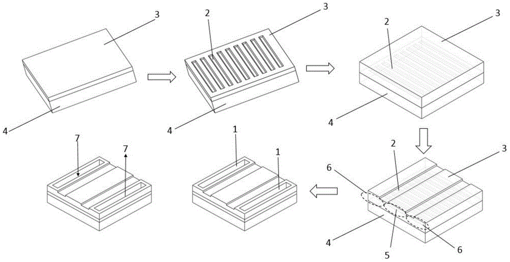
[0034] Such as image 3 As shown, the preparation method of the built-in nanochannel cooling terahertz quantum cascade semiconductor laser includes the following steps:
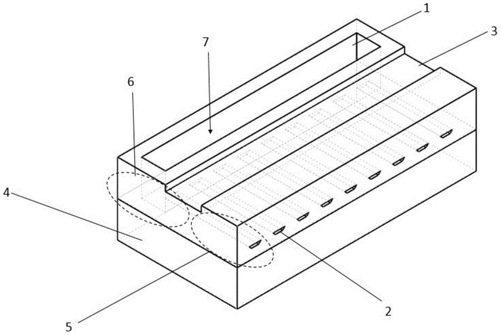
[0035] Step 1: On the part of the terahertz quantum cascade laser core layer 2 that has been grown and manufactured, by photolithography or electron beam exposure, prepare the exposure and etching according to the distribution of the designed built-in nanochannels 2, one-time A trench with a width of 300nm, a depth of 300nm, a sidewall inclination angle of 60°, and a trench length of 1200 μm was etched.
[0036] Step 2: The built-in nanochannel 3 is grown to form the built-in nanochannel 3 by using the growth rate of different crystal orientations by the method of secondary epitaxial growth, and the epitaxy is continued until the top surface is leveled, and then the core layer 3 of the terahertz quantum cascade laser is continued to be prepared.
[0037] Step 3: In the spanning length of 1.6mm, including pho...
Embodiment 2 and Embodiment 3
[0040] The preparation method of the built-in nano-channel cooling terahertz quantum cascade semiconductor laser comprises the following steps:
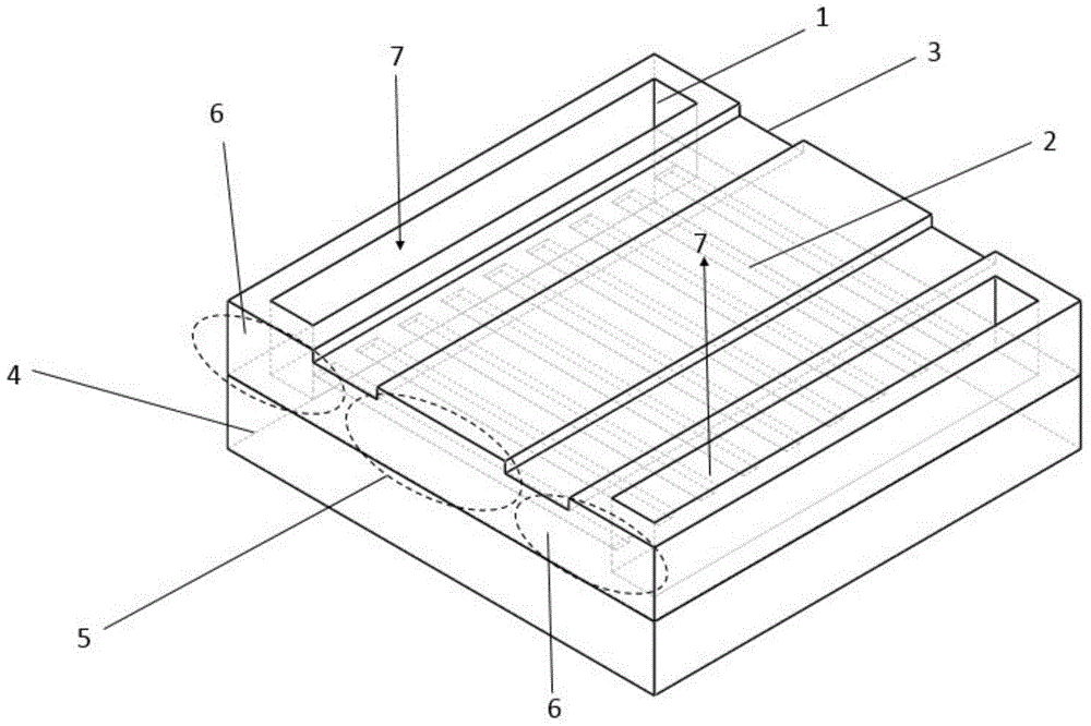
[0041] Step 1: On the substrate 4, by means of photolithography or electron beam exposure, prepare the distribution pattern of the designed built-in nanochannels 2 for exposure and etching, and etch the groove structure at one time.
[0042] Step 2, by secondary epitaxial growth, using the different growth rates of different crystal orientations, to grow and form the built-in nanochannel 3, and continue the epitaxy until the top surface of the substrate 4 is leveled, and then continue to prepare the terahertz quantum cascade laser core Layer 3.
[0043] Step 3, complete the usual semiconductor laser process steps such as photolithography, etching, making insulating layer, overlay, making electrode window, making P-side electrode, substrate thinning and optical sectioning, preparing N-side electrode, etc., to prepare terahertz quantum...
PUM
 Abstract
Description
Claims
Application Information
 - R&D
- Intellectual Property
- Life Sciences
- Materials
- Tech Scout
- Unparalleled Data Quality
- Higher Quality Content
- 60% Fewer Hallucinations
Browse by: Latest US Patents, China's latest patents, Technical Efficacy Thesaurus, Application Domain, Technology Topic, Popular Technical Reports.
© 2025 PatSnap. All rights reserved.Legal|Privacy policy|Modern Slavery Act Transparency Statement|Sitemap|About US| Contact US: help@patsnap.com


