Junction terminal structure of a thyristor chip
A junction terminal and thyristor technology, applied in the field of chip junction terminal structure, can solve the problems of forward and reverse voltage asymmetry, low withstand voltage, etc., and achieve the effect of increasing surface area, improving stability and reducing the gap
- Summary
- Abstract
- Description
- Claims
- Application Information
AI Technical Summary
Problems solved by technology
Method used
Image
Examples
Embodiment 1
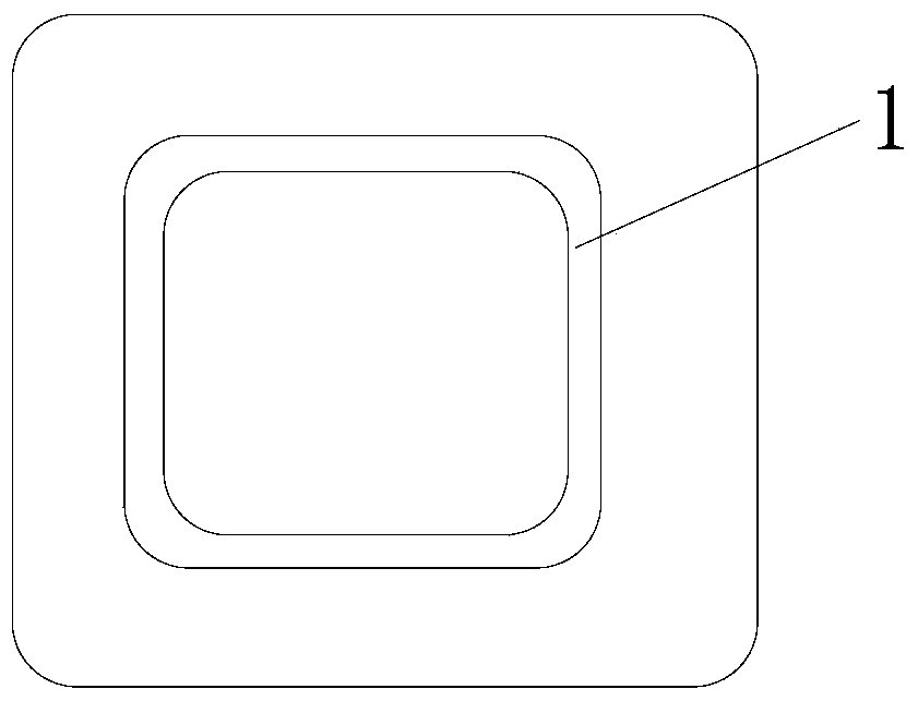
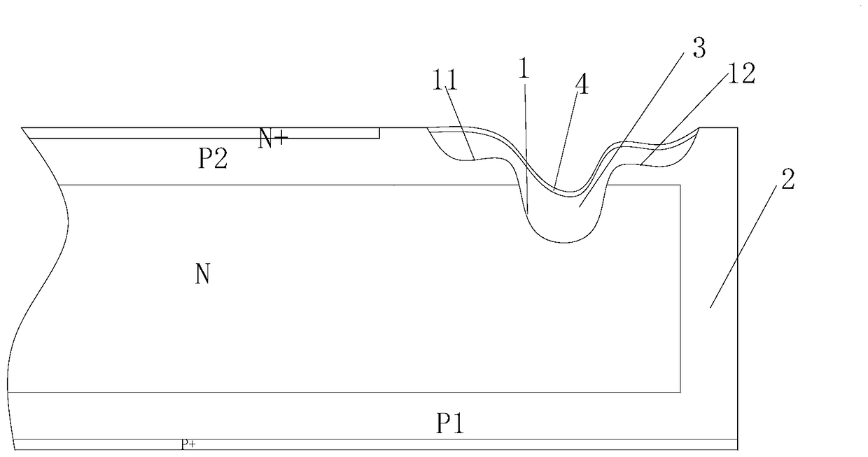
[0012] Embodiment 1: A junction terminal structure of a thyristor chip, such as figure 1 , figure 2 As shown, it includes long base area N, short base area P1, P2, isolation wall 2, phosphorus diffusion area N+, boron-concentrated diffusion area P+, voltage groove 1, and the voltage groove 1 is in a ring structure; the voltage groove 1 is a voltage tank structure with high voltage resistance and weak surface electric field. The depth of the voltage tank 1 is over P 2 The N junction extends into the long base region N20-70um. The inner surface of the voltage tank 1 is provided with an insulating layer 3 , and a glass passivation layer 4 is provided on the insulating layer. Take the designed thyristor chip with a peak theoretical withstand voltage of 2400V as an example:
[0013] When the traditional voltage tank structure is adopted, the peak withstand voltage is 1400V; when the one-step structure is adopted, the peak withstand voltage can reach 1900-2200V. The specific p...
Embodiment 2
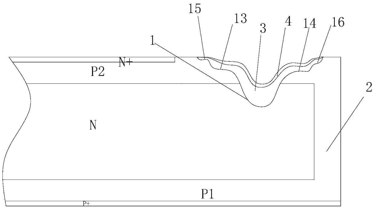
[0018] A junction termination structure of a thyristor chip, such as figure 1 , image 3 As shown, it includes long base area N, short base area P1, P2, isolation wall 2, phosphorus diffusion area N+, boron-concentrated diffusion area P+, voltage groove 1, and the voltage groove 1 is in a ring structure; the voltage groove 1 is a voltage tank structure with high voltage resistance and weak surface electric field. The depth of the voltage tank 1 is over P 2 The N junction extends into the long base region N20-70um. An insulating layer 3 is arranged on the inner surface of the voltage tank 1 , and a glass passivation layer 4 is arranged on the insulating layer 3 . Take the designed thyristor chip with a theoretical withstand voltage peak value of 3500V as an example:
[0019] When the traditional voltage tank structure is adopted, the peak withstand voltage is best at 1800V; when the one-level stepped structure is adopted, the peak withstand voltage is optimally 2800V, and w...
PUM
 Abstract
Description
Claims
Application Information
 - Generate Ideas
- Intellectual Property
- Life Sciences
- Materials
- Tech Scout
- Unparalleled Data Quality
- Higher Quality Content
- 60% Fewer Hallucinations
Browse by: Latest US Patents, China's latest patents, Technical Efficacy Thesaurus, Application Domain, Technology Topic, Popular Technical Reports.
© 2025 PatSnap. All rights reserved.Legal|Privacy policy|Modern Slavery Act Transparency Statement|Sitemap|About US| Contact US: help@patsnap.com


