Reverse-polarity AlGaInP light-emitting diode structure with window layer being covered with indium tin oxide

A technology of light-emitting diodes and indium tin oxide, which is applied in the direction of electrical components, circuits, semiconductor devices, etc., can solve the problems of inability to improve current expansion, inability to achieve ohmic contact, and increase the light output area of ​​the window layer, so as to improve light extraction efficiency, The effect of improving current expansion capability and significant cost-effective advantages

Inactive Publication Date: 2015-09-16
SHANDONG INSPUR HUAGUANG OPTOELECTRONICS
View PDF7 Cites 8 Cited by
  • Summary
  • Abstract
  • Description
  • Claims
  • Application Information

AI Technical Summary

Problems solved by technology

This invention is a two-dimensional application of ITO material in blue GaN light-emitting diodes. Its design cannot realize the ohmic contact in AlGaInP-based LEDs, and it does not involve the design of increasing the light output area of ​​the window layer.
[0007] International patent EP2337095A2 and related patent families disclose a GaN light-emitting diode structure design with ITO. Similar to the above, this invention is a two-dimensional application of ITO materials in blue GaN light-emitting diodes, and its design cannot be realized in AlGaInP-based LEDs. The ohmic contact in the system does not involve the design of increasing the light output area of ​​the window layer
[0008] U.S. Patent US20120043566Al and related patent families disclose a structure design of AlGaInP light-emitting diode with ITO. This patent applies ITO material to the dielectric layer in the mirror ODR structure, and does not involve the window layer application and perforation structure design proposed in this paper. , can not achieve the purpose of improving the current expansion and increasing the light output area of ​​the window layer
[0009] U.S. Patent US7018859B2 and related patent families disclose a flip-chip style AlGaInP light-emitting diode structure design with ITO. This patent applies ITO material to the epitaxial structure on the side of the solder layer, and does not involve the application of the window layer proposed in this paper. The perforated structure design cannot achieve the purpose of improving current expansion and increasing the light output area of ​​the window layer

Method used


Image

  • Reverse-polarity AlGaInP light-emitting diode structure with window layer being covered with indium tin oxide
  • Reverse-polarity AlGaInP light-emitting diode structure with window layer being covered with indium tin oxide

Examples


Embodiment 1

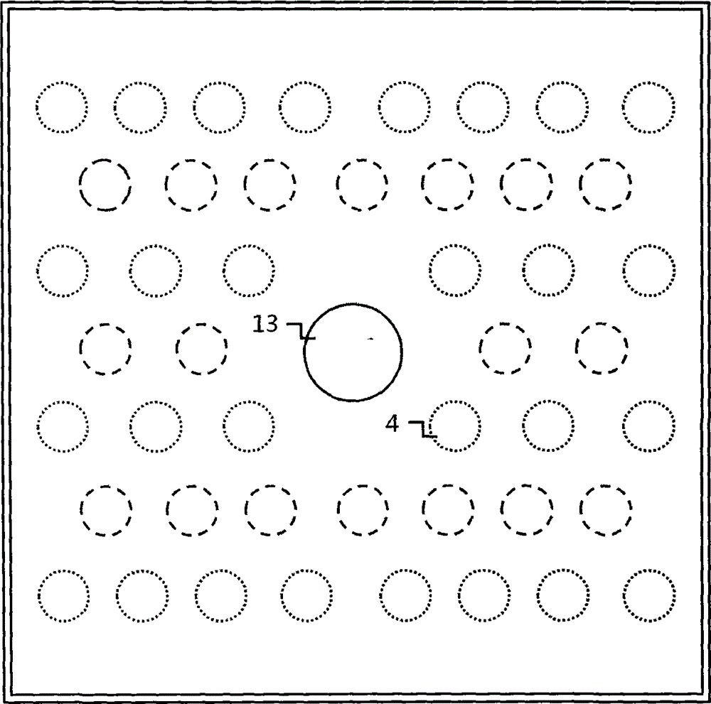
[0042] A reverse-polarity AlGaInP light-emitting diode structure with a window layer covered with indium tin oxide, the structure from bottom to top is p-electrode 1, substrate 2, bonding layer 3, mirror layer 4, insulating layer 5, current spreading Layer 6, p-type semiconductor layer 7, active region 8, n-type semiconductor layer 9, n-type semiconductor contact layer 10, window layer 11, indium tin oxide layer 12, n electrode 13; the indium tin oxide layer 12 covers The window layer 11 above the window layer 11 and penetrating the hole in the form of a cylinder is in direct contact with the n-type semiconductor contact layer 10 .

[0043] The p-electrode 1 is prepared on the back of the substrate 2, using a combination of Au and Ti materials, and prepared by evaporation, with a thickness of 0.5 μm;

[0044] The substrate 2 is made of Si material with a thickness of 20 μm;

[0045] The bonding layer 3 is made of Au material and prepared by evaporation, with a thickness of 0....

Embodiment 2

[0057] A kind of reverse polarity AlGaInP light-emitting diode structure that the window layer is covered with indium tin oxide as described in embodiment 1, and its difference is,

[0058] The p-electrode 1 is prepared on the back of the substrate 2, using a combination of Al and Ti materials, and prepared by evaporation, with a thickness of 1 μm;

[0059] The substrate 2 is made of Cu material with a thickness of 50 μm;

[0060] The bonding layer 3 is made of a combination of Au and In materials, prepared by evaporation, and has a thickness of 1 μm;

[0061] The reflector layer 4 is made of a combination of Ag, Ni, and Al materials, prepared by sputtering, and has a thickness of 0.5 μm;

[0062] Described insulating layer 5 selects TiO for use 2 The material is prepared by CVD with a thickness of 0.2 μm;

[0063] The current spreading layer 6 is a p-GaInP material prepared by MOCVD technology, and the p-type doping concentration is 1×10 19 cm -3 , with a thickness of 1 ...

Embodiment 3

[0072] A kind of reverse polarity AlGaInP light-emitting diode structure that the window layer is covered with indium tin oxide as described in embodiment 1, and its difference is,

[0073] The p-electrode 1 is prepared on the back of the substrate 2, using a combination of Ag, Ni, and Pt materials, and prepared by sputtering, with a thickness of 1 μm;

[0074] The substrate 2 is made of GaAs material with a thickness of 100 μm;

[0075] The bonding layer 3 is made of a combination of Al and Sn materials, prepared by evaporation, and has a thickness of 1.5 μm;

[0076] The reflector layer 4 is made of a combination of Au and Cr materials, prepared by sputtering, with a thickness of 1 μm;

[0077] The insulating layer 5 is made of Si 3 N 4 The material is prepared by CVD with a thickness of 0.5 μm;

[0078] The current spreading layer 6 is a p-GaAs material prepared by MOCVD technology, and the p-type doping concentration is 1×10 20 cm -3 , with a thickness of 2 μm;

[0...


PUM


Abstract

The invention provides a reverse-polarity AlGaInP light-emitting diode structure with a window layer being covered with an indium tin oxide (ITO). The structure sequentially comprises, from the bottom up, a p electrode, a substrate, a bonding layer, a reflector layer, an insulating layer, a current extension layer, a p-type semiconductor layer, an active region, an n-type semiconductor layer, an n-type semiconductor contact layer, the window layer, an indium tin oxide layer and an n electrode, wherein the indium tin oxide layer is covered on the window layer and runs through the window layer having openings in a cylinder form and is directly contacted with the n-type semiconductor contact layer. The structure can improve light extraction efficiency and current expansion efficiency of an LED chip and is easy to combine with the existing process.

Description

technical field [0001] The invention relates to a reverse polarity AlGaInP light-emitting diode structure whose window layer is covered with indium tin oxide, and belongs to the technical field of light-emitting diode manufacture. Background technique [0002] In the 1950s, with the efforts of many well-known research institutions represented by IBM Thomas J. Watson Research Center, III-V semiconductors represented by GaAs rose rapidly in the field of semiconductor light emitting. Later, with the emergence of metal-organic chemical vapor deposition (MOCVD) technology, the growth of high-quality III-V semiconductors broke through the technical barrier, and semiconductor light-emitting diode devices with various wavelengths flooded into the market one after another. Compared with the current light-emitting devices, semiconductor light-emitting diodes (LEDs) have the characteristics of high theoretical efficiency, long life, and mechanical shock resistance, and are regarded as ...

Claims


Application Information

Patent Timeline
Patent Type & Authority Applications(China)
IPC IPC(8): H01L33/42H01L33/38
CPCH01L33/42H01L33/20H01L33/38H01L33/58
Inventor 左致远夏伟陈康汤福国徐现刚
Owner SHANDONG INSPUR HUAGUANG OPTOELECTRONICS
Why Eureka
Try Eureka