Cob packaging process for integrated LED far and near light used in automobile headlights
A technology of automobile headlights and packaging technology, which is applied in the field of auto parts, can solve the problems of increasing the heat dissipation resistance of LED chips and unfavorable applications, and achieve the effects of being conducive to overall heat dissipation, compressing physical space and price costs, and improving heat dissipation channels
- Summary
- Abstract
- Description
- Claims
- Application Information
AI Technical Summary
Problems solved by technology
Method used
Image
Examples
Embodiment 1
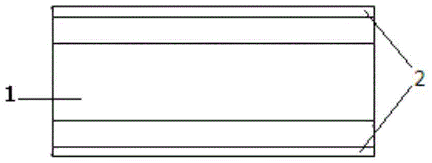
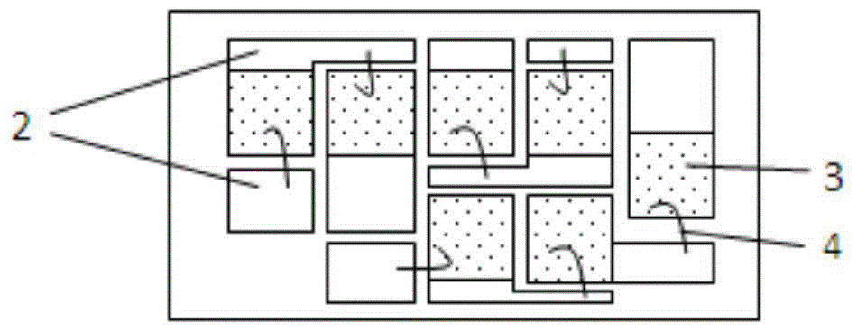
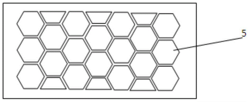
[0051] Such as Figure 5 As shown, the far and near light integrated LED light source module uses an aluminum nitride substrate with a thickness of 1.0mm. The front of the substrate is a copper foil layer with circuit functions. Strong bonding force and sufficient heat dissipation channels; the back of the substrate is a sheet of honeycomb copper foil layer, and the front and back copper foils of the substrate have gold-plated layers.
[0052] The number of LED chips for low beam and high beam in this light source are 4 and 7 respectively. The LED chip adopts a high-power chip with a vertical electrode structure. The negative electrode of the LED chip is fixed on a specific position in the front circuit of the aluminum nitride substrate by eutectic welding technology. The positive electrode of the LED chip is connected to the front of the substrate through a gold wire through a wire bonding process. In the circuit, realize the serial and parallel combined connection of LED ch...
Embodiment 2
[0056] Such as Figure 6 to Figure 8 As shown, the far and near light integrated LED light source module uses an alumina substrate with a thickness of 0.8mm. The front of the substrate is a copper foil layer with circuit functions. The copper foil layer is combined with aluminum nitride through high-temperature sintering, which has a good combination. The back of the substrate is a sheet of honeycomb copper foil layer, the front and back copper foils of the substrate have a gold-plated layer, and the copper foil on the front and back of the substrate is formed by the process of microporous copper paste and sintering. The path of morality.
[0057] The number of LED chips for low beam and high beam in this light source are 5 and 9 respectively. The LED chip adopts a high-power chip with a planar electrode structure. The back of the chip is gold-plated and can be fixed at a specific position in the front circuit of the alumina substrate through the eutectic welding process. The...
PUM
 Abstract
Description
Claims
Application Information
 - R&D Engineer
- R&D Manager
- IP Professional
- Industry Leading Data Capabilities
- Powerful AI technology
- Patent DNA Extraction
Browse by: Latest US Patents, China's latest patents, Technical Efficacy Thesaurus, Application Domain, Technology Topic, Popular Technical Reports.
© 2024 PatSnap. All rights reserved.Legal|Privacy policy|Modern Slavery Act Transparency Statement|Sitemap|About US| Contact US: help@patsnap.com


