


Quick Research
Generate reliable direction feasibility study reports for your R&D in just a few steps.

Technical Q&A
Discover and master advanced knowledge NOW. Basics, ideas, possibilities, all at once.

Find Solutions
As an expert in R&D theories, this can generate solutions to your technical problems instantly.

Evaluate Feasibility
Analyze your overall solution with one click, know your potential R&D risks in advance.

Monitor Landscape
Get weekly tech updates, stay abreast of the latest tech innovations and key insights.
Method for manufacturing semiconductor device
A manufacturing method and semiconductor technology, applied in semiconductor/solid-state device manufacturing, semiconductor devices, semiconductor lasers, etc., can solve problems such as device characteristics, reliability impact, inhalation of impurities, difficult growth conditions, etc., to improve device characteristics and reliability Effect
- Summary
- Abstract
- Description
- Claims
- Application Information
AI Technical Summary
Problems solved by technology
Method used
Image

Examples
Embodiment approach 1
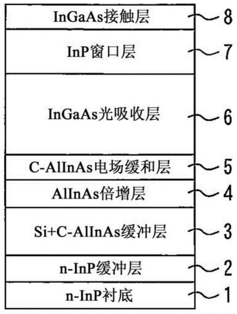
[0022] figure 1 It is a cross-sectional view showing the semiconductor device according to Embodiment 1 of the present invention. This semiconductor device is an avalanche photodiode as follows, that is, above an n-type InP substrate 1, layers having a carrier concentration of 3 to 5×10 18 cm -3 , an n-type InP buffer layer 2 with a thickness of 0.1-1 μm; a carrier concentration of 3-5×10 18 cm -3 , an n-type AlInAs buffer layer 3 with a thickness of 0.1-0.5 μm; an undoped AlInAs avalanche multiplication layer 4 with a thickness of 0.1-0.5 μm; a carrier concentration of 0.5-1×10 18 cm -3 , a p-type AlInAs electric field relaxation layer 5 with a thickness of 0.05-0.15 μm; a carrier concentration of 1-5×10 15 cm -3 , thickness 1 ~ 2μm n - Type InGaAs light absorbing layer 6; carrier concentration 0.01~0.1×10 15 cm -3 , thickness 0.5 ~ 1μm n - type InP window layer 7; and carrier concentration 1~5×10 18 cm -3 , a p-type InGaAs contact layer 8 with a thickness of 0.1-...
Embodiment approach 2
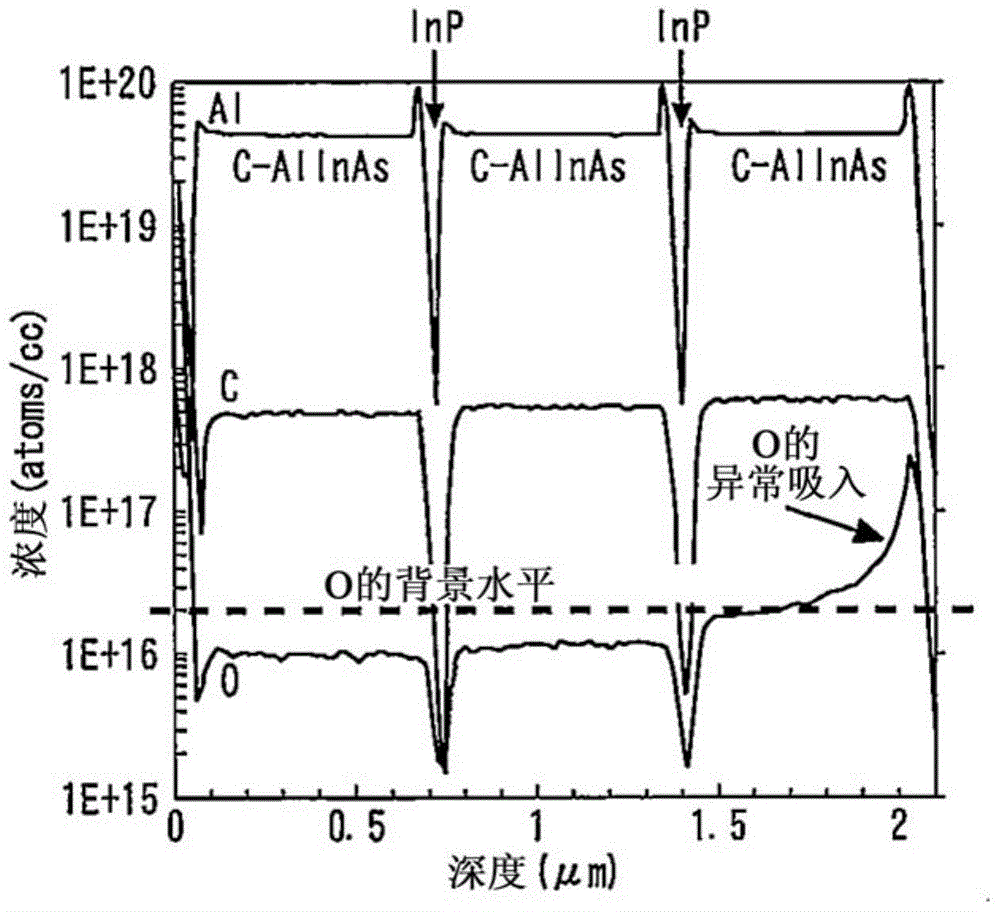
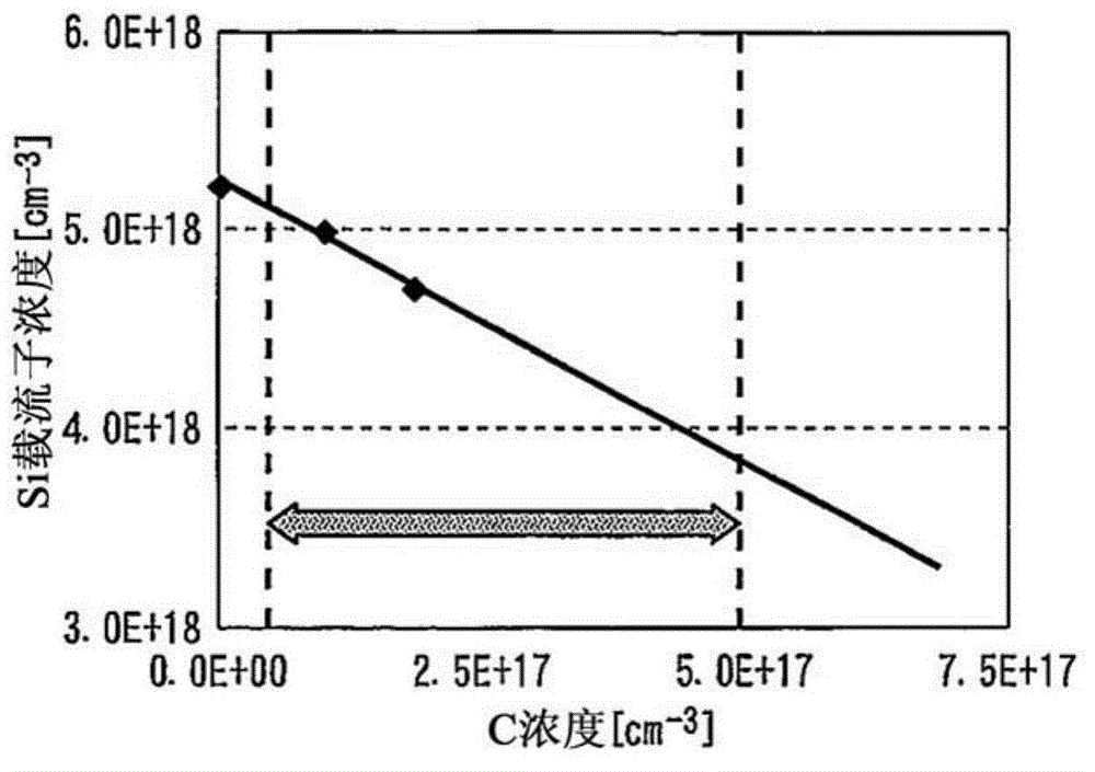
[0033] In Embodiment Mode 1, n-type AlInAs buffer layer 3 is doped with carbon using an organic halide to promote gettering. However, since carbon-doped AlInAs is p-type conduction, it inhibits n-type conduction by simultaneous doping of Si, and therefore it is necessary to control the carbon supply amount.
[0034] Therefore, in the present embodiment, carbon is doped together with Si in the n-type InP buffer layer 2 instead of the n-type AlInAs buffer layer 3 . If carbon is doped into InP, it shows n-type conduction. Therefore, since carbon functioning as an acceptor does not exist in the buffer layer, the impurity concentration control of the buffer layer becomes easy. In addition, impurities in the crystal growth furnace can be easily absorbed into InP. It is more difficult for impurities such as oxygen and carbon to be absorbed into InP than to be absorbed into AlInAs, so that the n-type InP buffer layer 2 having good crystallinity can be grown.
[0035] In addition, a...
Embodiment approach 3
[0037] In this embodiment, before forming the n-type InP buffer layer 2, CBr, which is a carbon additive material having a halogen as a constituent element, is added to 4 It is introduced into a crystal growth furnace, and the surface of n-type InP substrate 1 is etched and cleaned for 1 to 10 minutes. Thereafter, crystal growth is carried out in the same manner as in Embodiments 1 and 2.
[0038] The material introduced before growth is not just CBr 4 , can also be CCl 3 A carbon additive material having a halogen as a constituent element, such as Br (bromotrichloromethane), TBCl (terbium trichloride), or the like.
[0039] Alternatively, a material exhibiting a reducing action when thermally decomposed, such as an organometallic material containing Al (trimethylaluminum, etc.), may be introduced into the crystal growth furnace to reduce the surface of the n-type InP substrate 1 .
[0040] As described above, introducing a carbon additive material having a halogen in the c...
PUM
| Property | Measurement | Unit |
|---|---|---|
| thickness | aaaaa | aaaaa |
| thickness | aaaaa | aaaaa |
| thickness | aaaaa | aaaaa |
Abstract
Description
Claims
Application Information
 - R&D Engineer
- R&D Manager
- IP Professional
- Industry Leading Data Capabilities
- Powerful AI technology
- Patent DNA Extraction
Browse by: Latest US Patents, China's latest patents, Technical Efficacy Thesaurus, Application Domain, Technology Topic, Popular Technical Reports.
© 2024 PatSnap. All rights reserved.Legal|Privacy policy|Modern Slavery Act Transparency Statement|Sitemap|About US| Contact US: help@patsnap.com