Method for forming semiconductor device

A semiconductor and device technology, applied in the field of semiconductor device formation, can solve the problems of poor quality of stress layer and increased difficulty of stress layer, and achieve stable electrical performance and good quality

Inactive Publication Date: 2015-06-24
SEMICON MFG INT (SHANGHAI) CORP
View PDF5 Cites 2 Cited by
  • Summary
  • Abstract
  • Description
  • Claims
  • Application Information

AI Technical Summary

Problems solved by technology

[0004] However, as the process nodes of semiconductor devices continue to shrink, the size of the gate structure and the distance between adjacent gate structures also continue to shrink, making it more difficult to form a stress layer, and the quality of the formed stress layer deteriorates

Method used


Image

  • Method for forming semiconductor device
  • Method for forming semiconductor device
  • Method for forming semiconductor device

Examples


Embodiment Construction

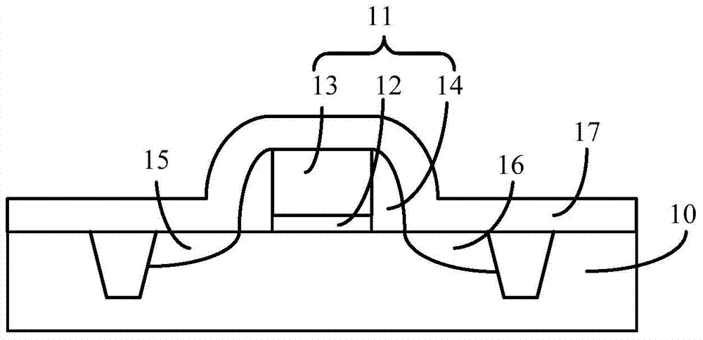
[0034] As mentioned in the background art, as the process nodes of semiconductor devices continue to shrink, the size of the gate structure and the distance between adjacent gate structures also continue to shrink, making it more difficult to form a stress layer, and the quality of the formed stress layer worse.

[0035] In order to expand the distance between adjacent gate structures and make the stress layer easy to fill the substrate surface between adjacent gate structures, a solution is to remove part of the sidewall (such as figure 1 shown) to increase the distance between adjacent gate structures, thereby reducing the aspect ratio (Aspect Ratio) of the trench between adjacent gate structures. Such as Figure 2 to Figure 5 Shown is a schematic cross-sectional structure diagram of the formation process of a transistor with a stress layer.

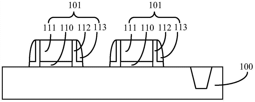
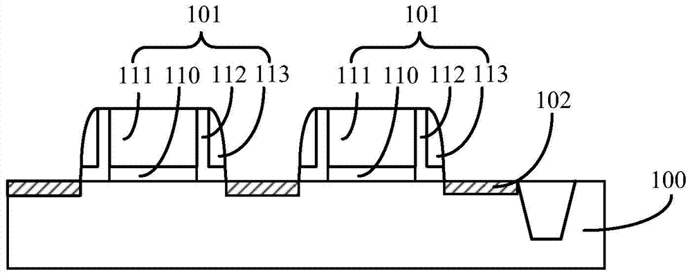
[0036] Please refer to figure 2 , provide a substrate 100, the surface of the substrate 100 has a plurality of gate structures 10...


PUM


Abstract

A method for forming a semiconductor device comprises the following steps: providing a substrate, wherein the substrate is provided with a plurality of gate structures on the surface, each gate structure is composed of a gate dielectric layer disposed on the surface of the substrate, a gate electrode layer disposed on the surface of the gate dielectric layer, side walls disposed at the two sides of the gate dielectric layer and the gate electrode layer, and first spacers on the surface of the substrate, and each first spacer is provided with a second spacer on the surface; removing the second spacers to expose the first spacers; forming a third spacer on the surface of each first spacer after the second spacers are removed; forming conductive layers on the surface of the substrate at the two sides of the third spacers and the gate structures by taking the third spacers and the gate structures as masks; and removing the third spacers after the conductive layers are formed, wherein no by-product is attached to the surfaces of the substrate, the conductive layers and the gate structures in the process for forming the third spacers. The performance of a semiconductor device formed by the method is improved.

Description

technical field [0001] The invention relates to the technical field of semiconductor manufacturing, in particular to a method for forming a semiconductor device. Background technique [0002] With the rapid development of semiconductor manufacturing technology, semiconductor devices are developing toward higher component density and higher integration in order to achieve higher computing speed, larger data storage capacity, and more functions. Therefore, the gates of Complementary Metal Oxide Semiconductor (CMOS) transistors are becoming thinner and shorter than before. However, the dimensional variation of the gate affects the electrical performance of the semiconductor device. At present, the performance of semiconductor devices is mainly improved by controlling the mobility of carriers. A key element of this technology is to control the stress in the transistor. By properly controlling the stress, the carriers (electrons in NMOS transistors and electrons in PMOS transist...

Claims


Application Information

Patent Timeline
Patent Type & Authority Applications(China)
IPC IPC(8): H01L21/336H01L21/28
CPCH01L29/665H01L29/7843
Inventor 刘佳磊
Owner SEMICON MFG INT (SHANGHAI) CORP
Why Eureka
Try Eureka