Thin film transistor, method for manufacturing the same, and display device

一种薄膜晶体管、制造方法的技术,应用在晶体管、半导体/固态器件制造、半导体器件等方向,能够解决成本提高、掩膜版数目增多、工艺复杂等问题,达到节省刻蚀时间、减少构图工艺次数、降低制造成本的效果

Active Publication Date: 2018-03-27
BOE TECH GRP CO LTD
View PDF3 Cites 1 Cited by
  • Summary
  • Abstract
  • Description
  • Claims
  • Application Information

AI Technical Summary

Problems solved by technology

Taking metal oxide TFT as an example, in theory, the manufacturing process of compound semiconductor TFT should be the same as that of amorphous silicon TFT, but in the existing technology, both dry etching and wet etching are vulnerable to chemical stability. The compound semiconductor active layer will cause damage and ultimately affect device performance, that is, the BCE process will damage the compound semiconductor active layer while forming the source and drain electrodes. Therefore, the current BCE process cannot be directly used to prepare compound semiconductor thin film transistors. Increase the preparation process of the etch stop layer used to protect the compound semiconductor active layer, but after adding the etch stop layer, the number of masks required for the preparation process will increase, the process will become complicated, and the cost will increase accordingly

Method used


Image

  • Thin film transistor, method for manufacturing the same, and display device
  • Thin film transistor, method for manufacturing the same, and display device
  • Thin film transistor, method for manufacturing the same, and display device

Examples


Embodiment

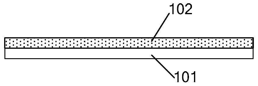
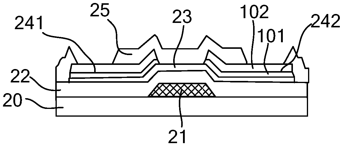
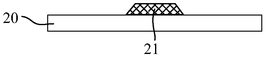
[0040] An embodiment of the present invention provides a thin film transistor, the thin film transistor includes: a gate electrode, an active layer, a source electrode and a drain electrode, the source electrode and the drain electrode are formed of at least two materials, and the source electrode and the drain electrode are formed of at least two materials. The forming material can undergo a battery reaction in the corresponding etching solution to be etched, and the etching solution does not corrode the active layer.

[0041] In view of the problem that the active layer of the existing TFT is easily corroded by the etching solution used in the source and drain formation processes, this embodiment adopts a new solution: the source and drain materials of the thin film transistor are selected to be suitable for A material that has a battery reaction in a certain electrolyte, and at the same time, the electrolyte corresponding to the battery reaction is used as an etching solutio...


PUM


Abstract

A thin film transistor, a manufacturing method thereof, and a display device are provided. The thin film transistor includes a gate electrode (21), an active layer (23), a source electrode (241) and a drain electrode (242). The source electrode (241) and the drain electrode (242) are formed of at least two materials, the forming materials of the source electrode (241) and the drain electrode (242) can create a cell reaction in a corresponding etching solution so as to be etched, and material of the active layer (23) is not corroded by the etching solution. With the thin film transistor and manufacturing method thereof according to embodiments of the invention, a problem that an active layer is liable to be corroded in an etching procedure of a source electrode and a drain electrode can be solved, and thus the thin film transistor device can be manufactured by using a back channel etch process. Consequently, the process number for manufacture of the thin film transistor is decreased, and the manufacturing cost is saved.

Description

technical field [0001] The present invention relates to the field of display, in particular to a thin film transistor, a method for manufacturing the same, and a display device. Background technique [0002] The thin film transistor TFT (Thin Film Transistor) with compound semiconductor represented by metal oxide as the active layer material has the advantages of high mobility, simple manufacturing process, good large area uniformity, and low manufacturing cost, and is considered to be the driving active matrix. Organic light-emitting diodes (Active Matrix Organic Light Emitting Diode, AMOLED) show the most potential devices. Therefore, compound semiconductor TFTs have attracted much attention in the industry in recent years, and have been gradually applied to AMOLED display panels. [0003] In the TFT manufacturing technology, the Back Channel Etch (BCE) process is a common process for amorphous silicon TFTs. It only takes four lithography to form the TFT: the first lithog...

Claims


Application Information

Patent Timeline
Patent Type & Authority Patents(China)
IPC IPC(8): H01L29/786H01L21/336H01L29/43
CPCH01L29/45H01L21/28575H01L21/32134H01L21/443H01L21/47635H01L29/20H01L29/2003H01L29/22H01L29/24H01L29/42356H01L29/66522H01L29/66742H01L29/66969H01L29/786H01L29/78681H01L29/7869
Inventor 王龙彦李永谦曹昆李全虎尹静文张保侠盖翠丽吴仲远王刚
Owner BOE TECH GRP CO LTD
Why Eureka
Try Eureka