


Quick Research
Generate reliable direction feasibility study reports for your R&D in just a few steps.

Technical Q&A
Discover and master advanced knowledge NOW. Basics, ideas, possibilities, all at once.

Find Solutions
As an expert in R&D theories, this can generate solutions to your technical problems instantly.

Evaluate Feasibility
Analyze your overall solution with one click, know your potential R&D risks in advance.

Monitor Landscape
Get weekly tech updates, stay abreast of the latest tech innovations and key insights.
Method and system for checking and analyzing repetitive photolithography defect of wafers, and wafer production method
A technology of defect inspection and analysis method, which is applied in the direction of semiconductor/solid-state device testing/measurement, electrical components, circuits, etc., and can solve the problems such as difficulty in effective detection of repetitive photolithography defects on wafers, easy missed detection or false detection, etc. Achieve the effect of reducing the risk of shipment, avoiding missed or false detection, and improving the yield
- Summary
- Abstract
- Description
- Claims
- Application Information
AI Technical Summary
Problems solved by technology
Method used
Image

Examples
Embodiment 1
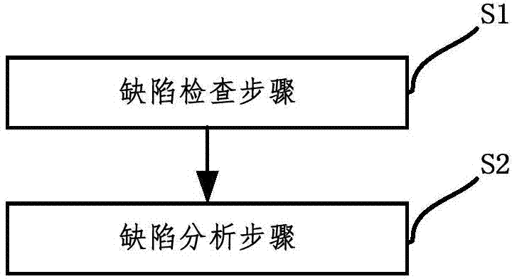
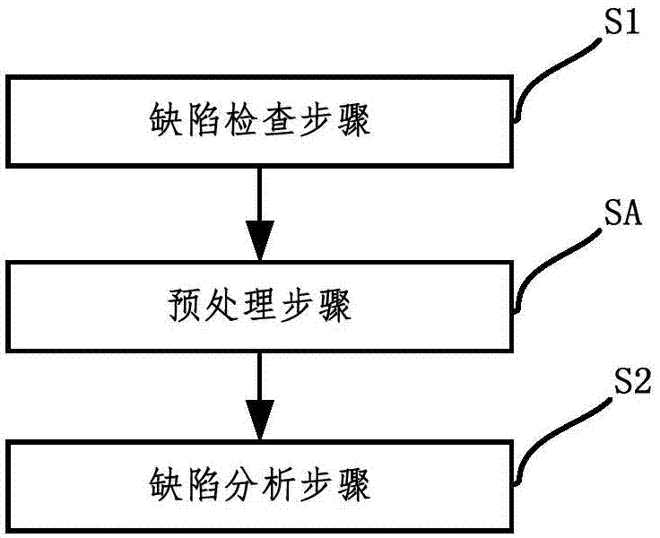
[0059] Such as figure 1 As shown, this example provides a method for inspection and analysis of wafer repetitive photolithography defects, including the following steps:
[0060] S1. Defect inspection step: After a certain batch of wafer photolithography process is completed, N wafers are selected from the batch of wafers, and the defects on the selected wafers are scanned in full to obtain the The defect information of the wafer is selected; the defect information includes the position information and size information of the defect;
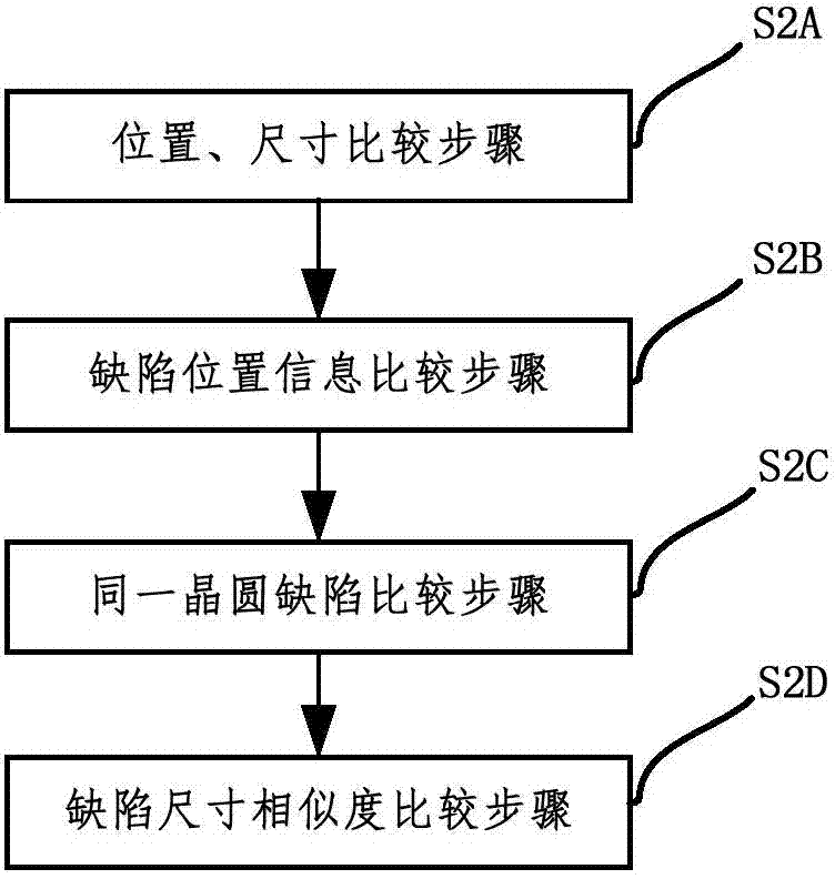
[0061] S2. Defect analysis step: comparing the position information and size information of the selected wafer defects;
[0062] If there are defects with consistent position information and size information on the selected wafers, it is determined that the batch of wafers has repetitive lithography defects in the lithography process;
[0063] If there is no defect with consistent position information on the selected wafer, it is determined th...
Embodiment 2
[0100] This example provides a wafer production method, including the following steps: after the photolithography process of a certain batch of wafers is completed, it is subjected to repetitive photolithography defect inspection and analysis;
[0101] If there is no repetitive photolithography defect, continue to follow-up production;
[0102] If there is a repetitive photolithography defect, the product will be treated as abnormal production, the photolithography process will be suspended, and production will continue after the repetitive photolithography defect is eliminated;
[0103] Wherein, the "performing inspection and analysis of repetitive photolithography defects" is realized by the wafer repetitive photolithography defect inspection and analysis method provided in Embodiment 1 above.
[0104] Regarding the above-mentioned wafer production method, most of the content is well known to those skilled in the art. The improvement of the present invention only improves it...
Embodiment 3
[0107] This example provides a wafer repetitive lithography defect inspection and analysis system, such as Figure 7 As shown, it includes the following modules:
[0108] The defect inspection module 1 is used to select N wafers from the batch of wafers after the photolithography process of a certain batch of wafers is completed, and perform full-chip scanning on the defects on the selected wafers to obtain the described Defect information of the selected wafer; the defect information includes position information and size information of the defect;
[0109] Defect analysis module 2, used to compare the position information and size information of the selected wafer defects;
[0110] If there are defects with consistent position information and size information on the selected wafers, it is determined that the batch of wafers has repetitive lithography defects in the lithography process;
[0111] If there is no defect with consistent position information on the selected wafe...
PUM
 Abstract
Description
Claims
Application Information
 - R&D Engineer
- R&D Manager
- IP Professional
- Industry Leading Data Capabilities
- Powerful AI technology
- Patent DNA Extraction
Browse by: Latest US Patents, China's latest patents, Technical Efficacy Thesaurus, Application Domain, Technology Topic, Popular Technical Reports.
© 2024 PatSnap. All rights reserved.Legal|Privacy policy|Modern Slavery Act Transparency Statement|Sitemap|About US| Contact US: help@patsnap.com