Manufacturing method of tunable quantum well laser epitaxial chips of large lattice mismatch

A technology of lattice mismatch and fabrication method, applied in lasers, phonon exciters, laser parts and other directions, can solve the problems of low height, carriers are easy to escape from potential wells, lasers cannot work stably, etc. Tuning to achieve a wide range of wavelengths

Active Publication Date: 2015-05-20
JIANGSU HUAXING LASER TECH CO LTD
View PDF5 Cites 4 Cited by
  • Summary
  • Abstract
  • Description
  • Claims
  • Application Information

AI Technical Summary

Problems solved by technology

For the quantum well of pure InAs material, the laser wavelength can only be adjusted by the thickness of the well layer. In order to obtain the InAs / InP quantum well material with a wavelength of 2 microns, the thickness of the InAs well layer must be lower than 2nm. Too thin quantum well With a large quantum size effect, the height of the quantum well band bottom energy level from the potential barrier is low, and the carriers are easy to escape from the potential well, causing the laser to not work stably

Method used


Image

  • Manufacturing method of tunable quantum well laser epitaxial chips of large lattice mismatch
  • Manufacturing method of tunable quantum well laser epitaxial chips of large lattice mismatch
  • Manufacturing method of tunable quantum well laser epitaxial chips of large lattice mismatch

Examples


Embodiment Construction

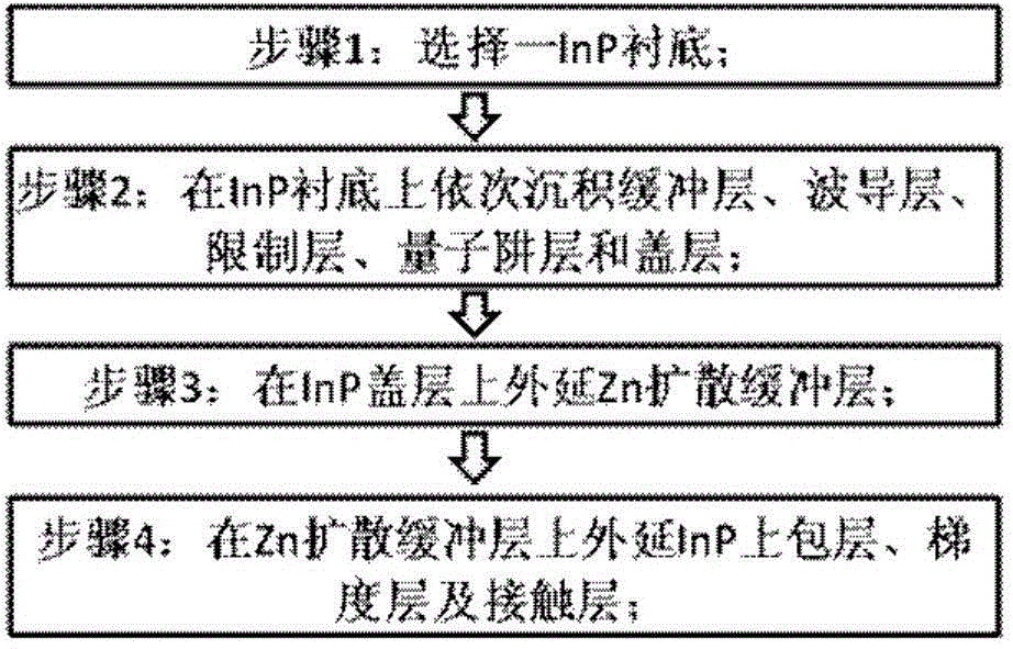
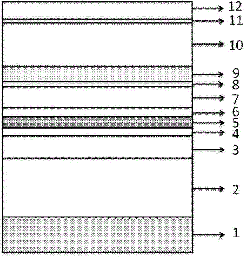
[0015] see figure 1 , figure 2 As shown, a method for manufacturing a large lattice mismatch tunable quantum well laser epitaxial chip of the present invention comprises the following steps:

[0016] Step 1: Select an InP substrate 1, wherein the InP substrate 1 is an InP single wafer, the crystal orientation is (001), the off angle is within ±0.5°, the thickness is 325-375 μm, and the doping concentration is (2-6) ×10 18 cm -3 ;

[0017] Step 2: On the substrate 1, deposit an InP buffer layer 2, a lower waveguide layer 3, a lower confinement layer 4, a quantum well layer 5, an upper confinement layer 6, an upper waveguide layer 7, and an InP capping layer 8; the InP buffer layer 2 The thickness is 500nm, the growth temperature is between 600 and 660°C, and the doping concentration is between 1×10 17 to 2×10 18 cm -3 Between, the growth rate is about 0.4-0.6nm / s, too fast growth rate is not conducive to the formation of high-quality buffer layer; wherein the material o...


PUM


Abstract

The invention discloses a manufacturing method of tunable quantum well laser epitaxial chips of the large lattice mismatch, which includes the following steps: step 1: selecting an InP (Indium Phosphide) substrate; sep 2: sequentially depositing an Inp buffer layer, a lower waveguide layer, a lower limiting layer, a quantum well layer, an upper limiting layer, an upper waveguide layer and an InP cover layer on the substrate; step 3: extending a Zn diffusion buffer layer from the InP cover layer; step 4: extending a Zn-doped InP upper cladding layer, a gradient layer and an InGaAs contact layer on the Zn diffusion buffer layer to complete the preparation. The manufacturing method of tunable quantum well laser epitaxial chips of the large lattice mismatch is capable of achieving a wide range of tune of the quantum well laser wavelength.

Description

technical field [0001] The invention belongs to the technical field of semiconductors, and in particular relates to the growth of a large mismatch In(Ga)As / InP quantum well material by molecular beam epitaxy (MBE) or metal organic chemical vapor deposition (MOCVD), through the introduction of a Zn diffusion buffer layer and precise regulation The Zn doping concentration of the laser cladding layer realizes the manufacturing method of the laser epitaxial chip with wide range of wavelength tunable. Background technique [0002] Since the advent of semiconductor lasers in the early 1960s, due to their performance advantages such as wide wavelength coverage, compact structure, high reliability and easy integration, they have been used in people's daily life, industrial and agricultural production, and national defense and military fields. be widely used. With the continuous expansion of emerging application fields, people have put forward new and higher requirements for the per...

Claims


Application Information

Patent Timeline
Patent Type & Authority Applications(China)
IPC IPC(8): H01S5/34H01S5/343
Inventor 罗帅季海铭杨涛
Owner JIANGSU HUAXING LASER TECH CO LTD
Why Eureka
Try Eureka