Photo-electrochemical hydrogen evolution electrode based on MoS2 and Ag modified silicon nanowire array and application thereof
A silicon nanowire array and photoelectrochemical technology, applied in the field of electrochemistry, can solve the problems of unsuitable hydrogen evolution materials and low hydrogen evolution efficiency, and achieve the effects of increased specific surface area, low oxidation degree, and increased probability
- Summary
- Abstract
- Description
- Claims
- Application Information
AI Technical Summary
Problems solved by technology
Method used
Image
Examples
Embodiment 1
[0024] Embodiment 1, preparation based on MoS 2 and Ag modified silicon nanowire array photoelectrochemical hydrogen evolution electrode
[0025] Using the Galvanic Displacement (Galvanic Displacement), the Ag-modified silicon nanowire arrays were prepared by the self-reduction of the silicon nanowire arrays prepared by the two-step metal-assisted catalytic etching method, and the Ag nanoparticles were modified on the silicon nanowire arrays, and then modified with Ag. Silicon nanowire arrays were used as substrate materials, and MoS 2 Reductive loading on the substrate to form MoS-based 2 and Ag-modified silicon nanowire arrays, and packaged as MoS 2 and Ag modified silicon nanowire array photoelectrochemical hydrogen evolution electrode, its specific implementation steps are as follows:
[0026] method 1:
[0027] (1) Two-step metal-assisted catalytic etching method to prepare silicon nanowire arrays: the silicon wafer was sequentially washed with deionized water, absolute...
Embodiment 2
[0039] Example 2, constructing MoS 2 Three-electrode system with Ag-modified silicon nanowire array photoelectrochemical hydrogen evolution electrode
[0040] in MoS 2 and Ag-modified silicon nanowire array; the electrode is the working electrode, the Ag / AgCl (saturated KCl) electrode is the reference electrode, the platinum sheet electrode is the counter electrode, and the connection circuit is designed according to the three-electrode system. Control the apparent area of the working electrode to 1 cm 2 , the electrolyte solution is containing 0.5M K 2 SO 4 and 0.1M H 2 SO 4 mixed aqueous solution. The experimental test conditions are atmospheric environment, the temperature is room temperature, the input power of the light source is 250W, and the wavelength range is 400-1200nm during the simulated sunlight illumination test.
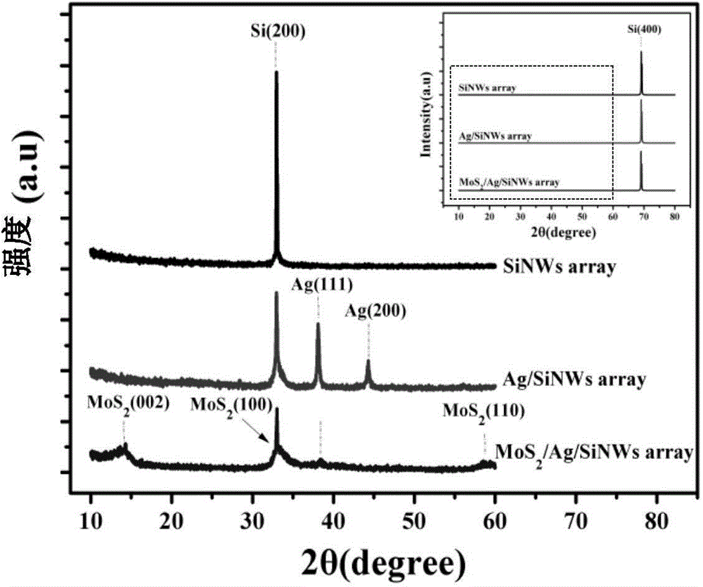
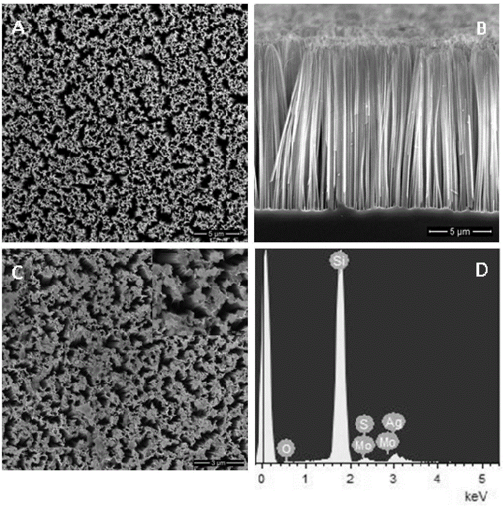
[0041] Then X-ray diffractometer (X-Ray Diffraction, XRD), field emission scanning electron microscope (Field Emission Scanning Electron micr...
PUM
| Property | Measurement | Unit |
|---|---|---|
| diameter | aaaaa | aaaaa |
| length | aaaaa | aaaaa |
| distance | aaaaa | aaaaa |
Abstract
Description
Claims
Application Information
 - R&D
- Intellectual Property
- Life Sciences
- Materials
- Tech Scout
- Unparalleled Data Quality
- Higher Quality Content
- 60% Fewer Hallucinations
Browse by: Latest US Patents, China's latest patents, Technical Efficacy Thesaurus, Application Domain, Technology Topic, Popular Technical Reports.
© 2025 PatSnap. All rights reserved.Legal|Privacy policy|Modern Slavery Act Transparency Statement|Sitemap|About US| Contact US: help@patsnap.com


