
Solvothermal preparation method of silicon-surface vertically-assembled CeO2 nanorod film

A technology of vertical assembly and nanorods, applied in chemical instruments and methods, inorganic chemistry, rare earth metal compounds, etc., can solve the problems of silicon wafer erosion, preparation of nano-CeO thin films, etc., and achieve simple equipment, high transparency of visible light, and wide application Effect

Inactive Publication Date: 2015-05-20
BOHAI UNIV
View PDF6 Cites 3 Cited by
  • Summary
  • Abstract
  • Description
  • Claims
  • Application Information

AI Technical Summary

Problems solved by technology

[0005] However, silicon wafers are severely corroded in the hydrothermal system, so nano-CeO cannot be prepared on the surface of silicon wafers by hydrothermal method. 2 film
At present, there is no use of solvothermal method to vertically assemble CeO on the surface of silicon wafers at home and abroad. 2 Reports on Nanorod Thin Films

Method used


Image

  • Solvothermal preparation method of silicon-surface vertically-assembled CeO2 nanorod film
  • Solvothermal preparation method of silicon-surface vertically-assembled CeO2 nanorod film
  • Solvothermal preparation method of silicon-surface vertically-assembled CeO2 nanorod film

Examples


preparation example Construction

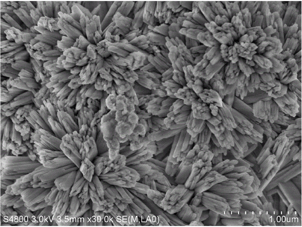
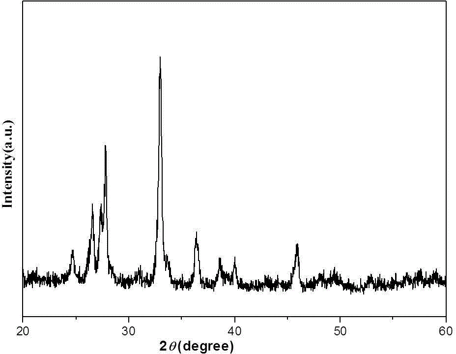
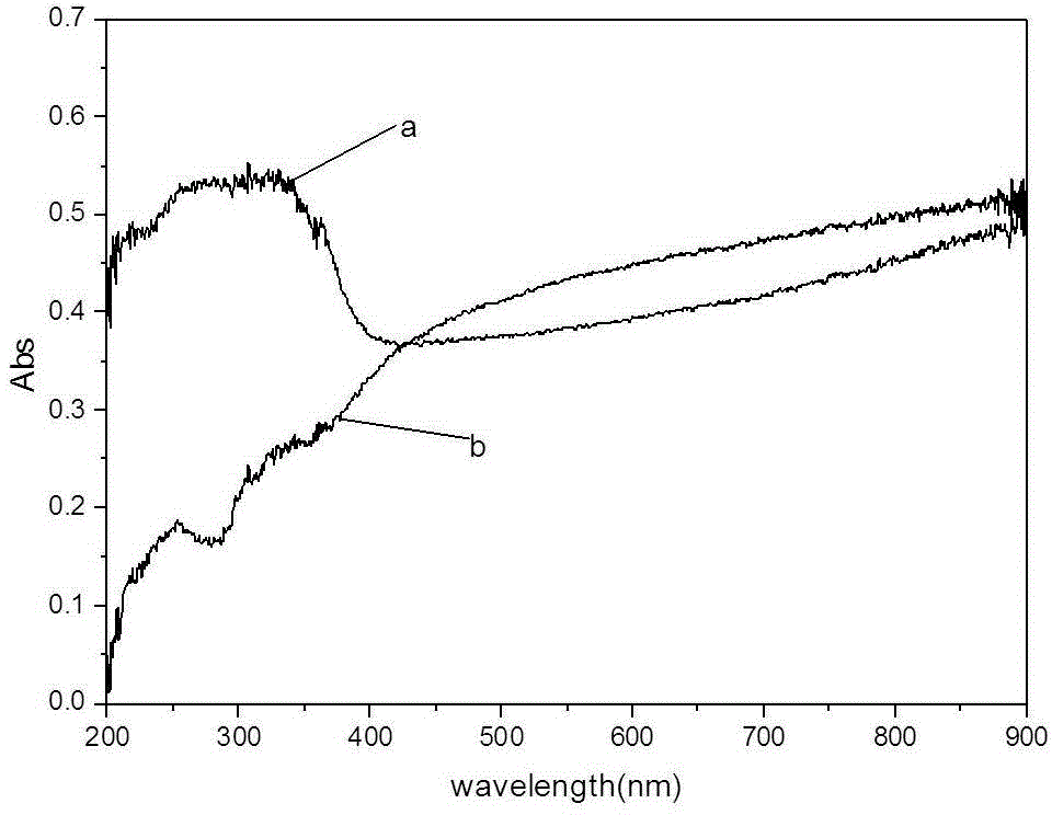
[0022] The invention provides a kind of silicon surface vertical assembly CeO 2 The solvothermal preparation method of nanorod film has simple equipment, low film production cost, no need for high temperature treatment of silicon substrate and film, and CeO with strong ultraviolet absorption ability and strong luminescence 2 Nanorods are assembled on a silicon wafer, and the resulting film is made of CeO 2 (The XRD spectrum of the film is as figure 2 shown) nanorods assembled vertically (SEM photo of the film is shown in figure 1 shown), uniform, high transparency of visible light, good adhesion, strong UV resistance (UV spectrum as shown image 3 shown), and has a strong emission peak at 380-390nm (the emission spectrum is shown in Figure 4 Shown), it is widely used in the anti-ultraviolet performance of crystalline silicon solar cells. CeO assembled vertically on silicon wafer surface 2 The nanorod film has a diameter of 30-50nm, a film thickness of about 170 nm, a go...

Embodiment 1

[0030] Feed CeCl 3 ·7H 2 O is dissolved in absolute ethanol to obtain 0.01mol / L CeCl 3 solution in absolute ethanol, add 0.02mol / L CO(NH 2 ) 2 , urea and CeCl 3 The molar ratio of the mixture is 2:1, and the mixture is evenly stirred to obtain a precursor solution. Put the clean silicon wafer into a polytetrafluoroethylene-lined reactor, add the precursor solution (filling degree is 70%), seal it, place it in an oven, and react at 200°C for 3 hours. After the reaction is finished, the silicon chip is taken out after naturally cooling down to room temperature, washed with ethanol and water respectively, and dried to obtain the product.

Embodiment 2

[0032] Feed CeCl 3 ·7H 2 O is dissolved in absolute ethanol to obtain 0.015mol / LCeCl 3 solution in absolute ethanol, add 0.03mol / L CO(NH 2 ) 2 , urea and CeCl 3 The molar ratio of the mixture is 2:1, and the mixture is evenly stirred to obtain a precursor solution. Put the clean silicon wafer into a polytetrafluoroethylene-lined reactor, add the precursor solution (filling degree is 70%), seal it, place it in an oven, and react at 180°C for 4 hours. After the reaction is finished, the silicon chip is taken out after naturally cooling down to room temperature, washed with ethanol and water respectively, and dried to obtain the product.


PUM

PropertyMeasurementUnit
diameteraaaaaaaaaa
lengthaaaaaaaaaa
diameteraaaaaaaaaa

Abstract

The invention relates to a solvothermal preparation method of a silicon-surface vertically-assembled CeO2 nanorod film, which comprises the following steps: preparing a precursor solution by using ethanol as a solvent, and reacting the raw materials CeCl3 and CO(NH2)2 under the solvothermal conditions of 160-200 DEG C by using a clean silicon chip as a base to prepare the film formed by vertically assembling CeO2 nanorods on the silicon chip surface. The method has the advantages of simple equipment and low film-preparation cost, and does not need to perform high-temperature treatment on the silicon base and film. The prepared film is vertically assembled from the CeO2 nanorods, is thin and uniform, has the advantages of high visible light transparency, favorable adhesiveness and high ultraviolet resistance, has very strong emission peak at 380-390nm, and has wide application prospects in the aspect of crystalline silicon solar cell ultraviolet resistance.

Description

Technical field [0001] The invention involves a vertical assembly CEO on the silicon barrier 2 The solvent heat preparation method of nano -stick film belongs to the research technology field of new structured nanomaterials. Background technique [0002] In high altitude areas, due to the thin and ultraviolet rays of the ozone, solar cells with average life span of about 15 years are reduced, and the service life of high altitude areas has been reduced to about 5 years.Add an effective way to increase the life of solar cells on the surface of solar cells to increase the service life of solar cells. On the other hand, for crystalline silicon solar cells, 43%of the total energy of solar light cannot be absorbed and used.Light can also have a shielding function material for ultraviolet rays.Nano CEO 2 The advantages of visible light transmission and high ultraviolet absorption capacity have attracted much attention. [0003] Zou Yunling and others (Egg Trumin Auxiliary Water Heat La...

Claims


Application Information

Patent Timeline
Patent Type & Authority Applications(China)
IPC IPC(8): C01F17/00C04B41/50
Inventor 刘连利孙彤王莉丽崔岩张帆孙志佳
Owner BOHAI UNIV
Learn More