Packaging substrate and manufacturing method thereof

A technology for packaging substrates and manufacturing methods, which is applied in the fields of printed circuit manufacturing, multilayer circuit manufacturing, semiconductor/solid-state device manufacturing, etc., can solve problems such as packaging structure thickness reduction obstacles, improve production efficiency, save manufacturing process time, Effect of Thin Package Thickness

Active Publication Date: 2015-04-29
SUBTRON TECH
View PDF3 Cites 4 Cited by
  • Summary
  • Abstract
  • Description
  • Claims
  • Application Information

AI Technical Summary

Problems solved by technology

Therefore, if the thickness of the core dielectric layer cannot be effectively reduced, it will inevitably cause great obstacles in reducing the thickness of the packaging structure.

Method used


Image

  • Packaging substrate and manufacturing method thereof
  • Packaging substrate and manufacturing method thereof
  • Packaging substrate and manufacturing method thereof

Examples


Embodiment Construction

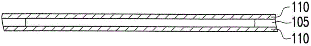
[0040] Figure 1A to Figure 1H is a schematic cross-sectional view of manufacturing process steps of a packaging carrier according to an embodiment of the present invention. In this embodiment, the manufacturing method of the packaging carrier includes the following steps: first, please refer to Figure 1A , bonding the two base metal layers 110 . In this embodiment, the two base metal layers 110 can be two copper foil layers respectively, and the two base metal layers 110 are bonded by coating the adhesive layer 105 on the periphery of the two base metal layers 110, and the two base metal layers 110 The peripheries of the two base metal layers 110 form a bonding area to temporarily bond the two base metal layers 110 together, so as to prevent the chemicals used in the subsequent manufacturing process from penetrating between the two base metal layers 110 .

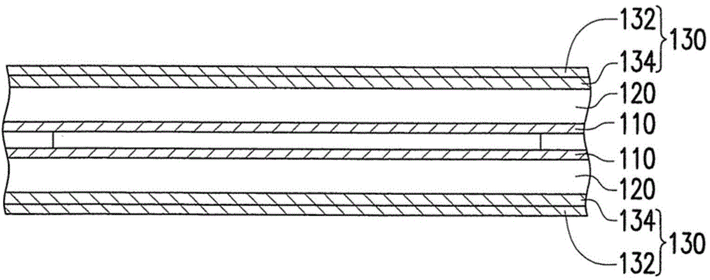
[0041] Please continue to refer to Figure 1B , press and bond the two support layers 120 on the two base metal layer...


PUM

PropertyMeasurementUnit
widthaaaaaaaaaa
widthaaaaaaaaaa
thicknessaaaaaaaaaa

Abstract

The invention discloses a manufacturing method for a packaging substrate. The method comprises the following steps: jointing two substrate metal layers; pressing two supporting layers on the substrate metal layers respectively; arranging two release metal films on the supporting layers respectively, wherein each release metal film comprises a first metal foil layer and a second metal foil layer which can be separated from each other; forming two first patterned metal layers on the release metal films respectively, wherein each first patterned metal layer comprises a connecting pad pattern; forming two dielectric layers on the release metal films respectively and covering the corresponding first patterned metal layers, wherein a conducting hole is formed in each dielectric layer and the dielectric layers are connected with the corresponding connecting pad patterns respectively; forming two second patterned metal layers on the dielectric layers respectively, wherein the second patterned metal layers at least cover the upper surfaces of the corresponding conducting holes; separating the substrate metal layers to form two packaging substrates independent of each other.

Description

technical field [0001] The present invention relates to a packaging structure and a manufacturing method thereof, and in particular to a packaging carrier board and a manufacturing method thereof. Background technique [0002] The purpose of chip packaging is to protect the bare chip, reduce the density of chip contacts and provide good heat dissipation for the chip. A common packaging method is to mount the chip on the package substrate through wire bonding or flip chip bonding, so that the contacts on the chip can be electrically connected to the package substrate. Therefore, the contact distribution of the chip can be reconfigured through the package substrate to conform to the contact distribution of the next level of external components. [0003] Generally speaking, the production of package substrates usually uses the core (core) dielectric layer as the core material, and uses the fully additive process (fully additive process), semi-additive process (semi-additive pr...

Claims


Application Information

Patent Timeline
Patent Type & Authority Applications(China)
IPC IPC(8): H01L21/48H01L23/498H05K3/46H05K1/00H05K1/02
CPCH01L2224/48091H01L2224/48227H01L2224/48465H01L2924/15311H01L2924/181H01L2924/00014H01L2924/00012H01L2924/00H01L21/4871H01L23/49822H05K1/00H05K1/02H05K3/4644
Inventor 孙世豪
Owner SUBTRON TECH
Why Eureka
Try Eureka