
PMOS device and preparation method thereof

A device and seed layer technology, applied in the field of semiconductor technology, can solve the problems of device performance degradation, aggregation interface, easy to generate defects, etc., and achieve the effect of reducing resistance, uniform distribution, and improving hole mobility

Active Publication Date: 2015-04-29
SEMICON MFG INT (SHANGHAI) CORP
View PDF4 Cites 8 Cited by
  • Summary
  • Abstract
  • Description
  • Claims
  • Application Information

AI Technical Summary

Problems solved by technology

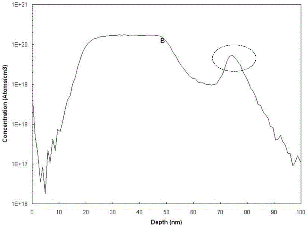
[0007] In view of the above-mentioned shortcomings of the prior art, the object of the present invention is to provide a PMOS device and a preparation method thereof, which are used to solve the problems caused by the accumulation of boron atoms at the interface of Si and SiGe in the prior art and the easy generation of defects at the interface, etc. The problem of slow performance

Method used


Image

  • PMOS device and preparation method thereof
  • PMOS device and preparation method thereof
  • PMOS device and preparation method thereof

Examples


Embodiment 1

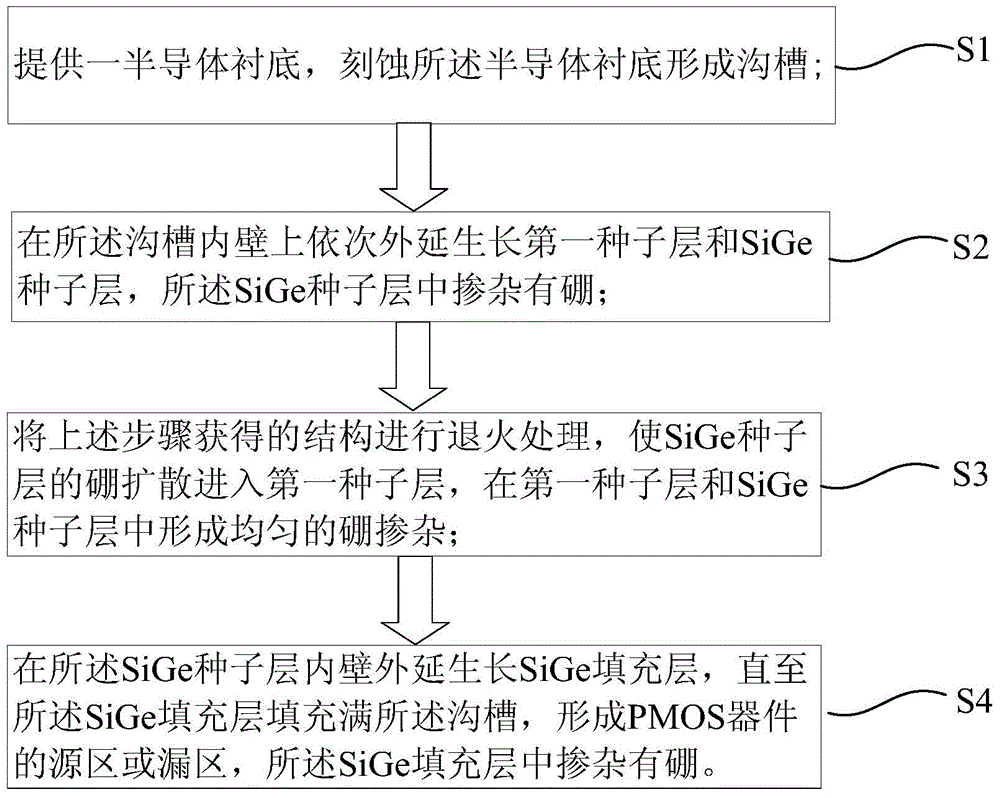
[0044] Such as figure 2 As shown, the present invention provides a kind of preparation method of PMOS device, and the preparation method of described PMOS device comprises the following steps at least:

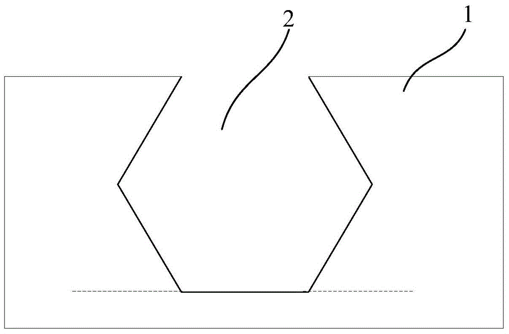
[0045] First execute step S1, such as image 3 As shown, a semiconductor substrate 1 is provided, and the semiconductor substrate is etched to form a trench 2 .

[0046] The semiconductor 1 substrate can be any known semiconductor substrate, including but not limited to Si substrate or SOI substrate. In this embodiment, the semiconductor substrate 1 is described by taking a Si substrate as an example.

[0047]The trench 2 can be formed by using known techniques, for example, dry etching, wet etching and the like. The shape of the trench 2 formed includes but not limited to a sigma shape, ie a “Σ” shape. Certainly, the groove 2 may also be in the shape of a rectangle, an inverted trapezoid, etc. as required. In this embodiment, the shape of the trench 2 is a “Σ” shape to ...

Embodiment 2

[0073] The present invention also provides a PMOS device, which is made by the preparation method in Embodiment 1, such as Figure 6 As shown, the PMOS device includes at least:

[0074] A semiconductor substrate 1, in which a trench 2 is formed by etching;

[0075] A first seed layer 3 containing uniform boron doping is epitaxially extended on the inner wall of the trench 2;

[0076] A SiGe seed layer 4 containing uniform boron doping is epitaxial on the inner wall of the first seed layer 3;

[0077] The SiGe filling layer 5 is epitaxial on the inner wall of the SiGe seed layer 4 and fills the trench 2 , and the SiGe filling layer 5 is doped with boron.

[0078] Preferably, the groove 2 is in a "Σ" shape. Certainly, the groove 2 may also be in the shape of a rectangle, an inverted trapezoid, etc. as required. In this embodiment, the shape of the trench 2 is a “Σ” shape to enhance the compressive stress effect of the SiGe filling layer subsequently formed in the trench 2 ....


PUM

PropertyMeasurementUnit
thicknessaaaaaaaaaa
thicknessaaaaaaaaaa
thicknessaaaaaaaaaa

Abstract

The invention provides a PMOS device and a preparation method thereof. The preparation method at least includes the following steps: forming a groove in a semiconductor substrate; sequentially growing a first seed layer and a SiGe seed layer in an epitaxial manner on the inner wall of the groove, wherein boron is doped in the SiGe seed layer; annealing the obtained structure, enabling boron in the SiGe seed layer to diffuse in the first seed layer, and forming uniform boron doping in the first seed layer and the SiGe seed layer; growing a SiGe filling layer until a source region or drain region formed by the groove, of the PMOS device is filled with the SiGe filling layer, wherein the SiGe filling layer is doped with boron. According to the invention, acceptor doped ions in the SiGe seed layer diffuse in the first seed layer through the annealing process, so as to be uniformly distributed in the SiGe seed layer and the first seed layer, as a result, accumulation of doped ions at the Si and SiGe interfaces is avoided, resistance at the source region and the drain region is reduced, and improvement on hole mobility is facilitated.

Description

technical field [0001] The invention relates to the field of semiconductor technology, in particular to a PMOS device and a preparation method thereof. Background technique [0002] Metal-oxide-semiconductor field-effect transistor (MOSFET) is the most important basic active device of integrated circuits, and CMOS, which is formed by complementing NMOS and PMOS, is the constituent unit of deep submicron ultra-large integrated circuits. Among them, Si CMOS integrated circuits occupy a dominant position in the semiconductor integrated circuit industry due to their advantages of low power consumption, high integration, low noise and high reliability. However, with the further increase of the scale of integrated circuits, the reduction of device feature size, the increase of integration and complexity, especially after the device feature size enters the nanometer scale, the limitations of materials and physical characteristics of Si CMOS devices have gradually emerged. out, lim...

Claims


Application Information

Patent Timeline
Patent Type & Authority Applications(China)
IPC IPC(8): H01L21/336H01L29/78H01L29/06
CPCH01L21/02694H01L29/66477H01L29/78
Inventor 林静
Owner SEMICON MFG INT (SHANGHAI) CORP
Learn More