A kind of multi-layer printed circuit board and its manufacturing method
A technology of multi-layer printing and production method, which is applied in the direction of multi-layer circuit manufacturing, printed circuit manufacturing, printed circuit, etc., can solve the problems of multi-layer printed circuit board scrapping, water vapor cannot be effectively discharged, etc., and achieve the goal of reducing the board explosion rate Effect
- Summary
- Abstract
- Description
- Claims
- Application Information
AI Technical Summary
Problems solved by technology
Method used
Image

Examples
Embodiment 1
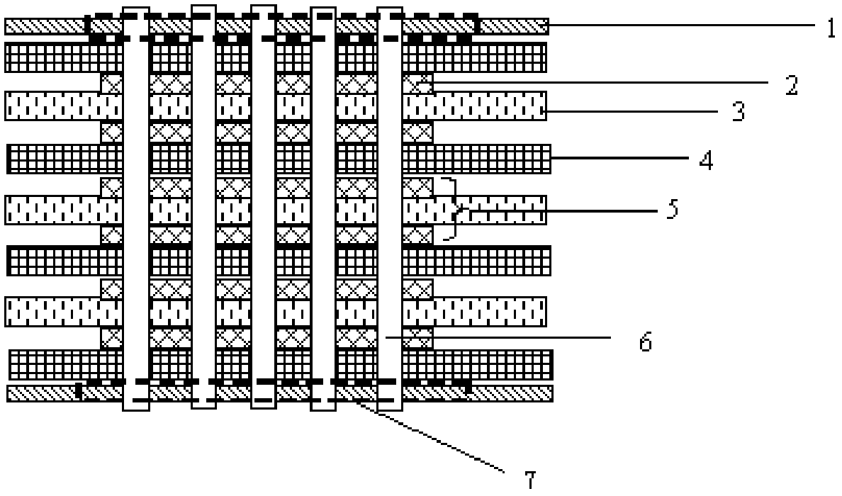
[0030] Such as figure 1 , figure 2 As shown, this embodiment provides a multilayer printed circuit board, including: at least two layers of inner core board 3 and copper foil 1, the inner core board 3 and the copper foil 1 are stacked, and the inner layer The core board 3 is provided with a hot-melt area 2, and the hot-melt area 2 is provided with a dielectric layer formed after the melted prepreg 4 is solidified and filled into the hot-melt area 2 after the melt process. The printed circuit board also includes: the circuit pattern area in contact with the dielectric layer in the hot-melt area 2 is provided with at least one explosion-proof groove 6, and the explosion-proof groove 6 runs through and contacts the dielectric layer in the hot-melt area 2 The circuit pattern area, the inner core board 3 and the copper foil 1. The above-mentioned multilayer printed circuit board is positioned through the dielectric layer formed by curing through the melt glue process, and then t...
Embodiment 2
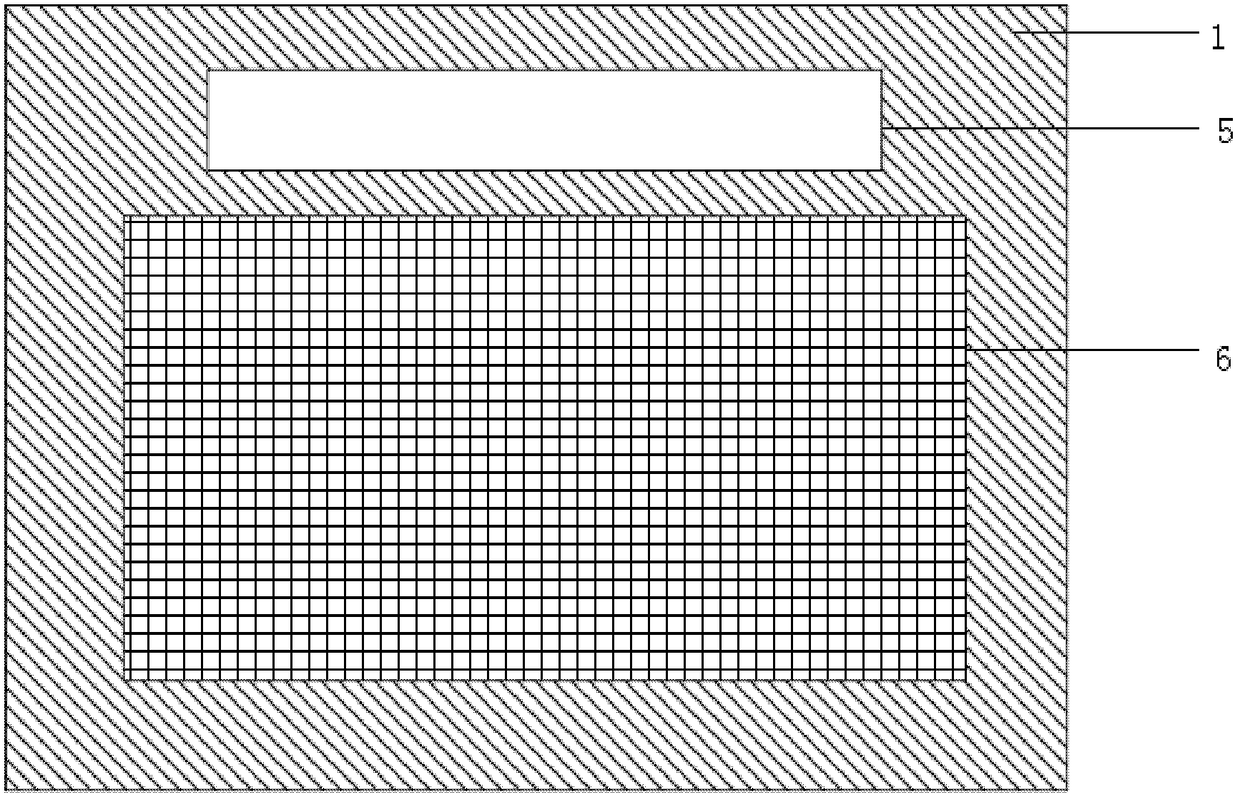
[0044] Such as image 3 As shown, this embodiment provides a multilayer printed circuit board, including: at least two layers of inner core board 3 and copper foil 1, the inner core board 3 and the copper foil 1 are stacked, and the inner layer The core board 3 is provided with a hot-melt area 2, and the hot-melt area 2 is provided with a dielectric layer formed after the melted prepreg 4 is solidified and filled into the hot-melt area 2 after the melt process. The multi-layer printing The circuit board is formed by laminating and laminating the inner core board 3, the prepreg 4, and the copper foil 1. The multilayer printed circuit board also includes: the dielectric layer in the hot-melt area 2 and the At least one explosion-proof groove 6 is jointly arranged between the circuit pattern areas in contact with the dielectric layer in the hot-melt area 2, and the explosion-proof groove 6 runs through the dielectric layer in the hot-melt area 2 and connects with the hot-melt Th...
Embodiment 3
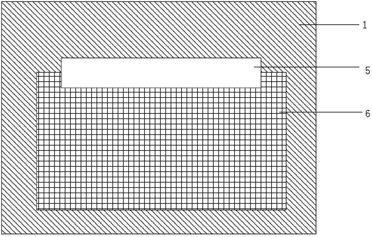
[0051] Such as Figure 4 As shown, this embodiment provides a multilayer printed circuit board, including: at least two layers of inner core board 3 and copper foil 1, the inner core board 3 and the copper foil 1 are stacked, and the inner layer The core board 3 is provided with a hot-melt area 2, and the hot-melt area 2 is provided with a dielectric layer formed after the melted prepreg 4 is solidified and filled into the hot-melt area 2 after the melt process. The multi-layer printing The circuit board is laminated by the inner core board 3, the prepreg 4, and the copper foil 1, and then laminated. The multilayer printed circuit board also includes: the dielectric layer in the hot-melt area 2 is provided with at least An explosion-proof groove 6 , the explosion-proof groove 6 runs through the dielectric layer in the hot-melt area 2 , the inner core board 3 and the copper foil 1 .
[0052] Preferably, an etching window 7 is provided corresponding to the outer circuit pattern...
PUM
 Abstract
Description
Claims
Application Information
 - Generate Ideas
- Intellectual Property
- Life Sciences
- Materials
- Tech Scout
- Unparalleled Data Quality
- Higher Quality Content
- 60% Fewer Hallucinations
Browse by: Latest US Patents, China's latest patents, Technical Efficacy Thesaurus, Application Domain, Technology Topic, Popular Technical Reports.
© 2025 PatSnap. All rights reserved.Legal|Privacy policy|Modern Slavery Act Transparency Statement|Sitemap|About US| Contact US: help@patsnap.com