
Reversed stack MTJ

A device, integrated circuit technology, applied in the field of inverted MTJ stacks

Active Publication Date: 2015-03-18
TAIWAN SEMICON MFG CO LTD
View PDF11 Cites 22 Cited by
  • Summary
  • Abstract
  • Description
  • Claims
  • Application Information

AI Technical Summary

Problems solved by technology

These memory types are volatile: only power is supplied to refresh the capacitor charges in DRAM and to keep the transistors in SRAM turned on to store data

Method used


Image

  • Reversed stack MTJ
  • Reversed stack MTJ
  • Reversed stack MTJ

Examples


Embodiment Construction

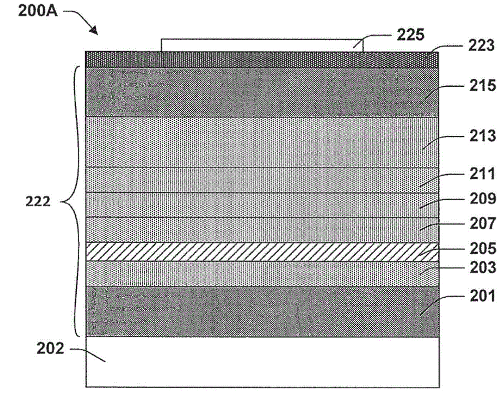
[0033] The inventors realized that conventional manufacturing processes can lead to defects in MRAM cells. In particular, it has been found that the free layer is susceptible to plasma damage and metal ion contamination during etching. The inventors solved the above problem by reversing the conventional order of thin film stacking to place the free layer at the bottom. This makes it easy to etch the free layer separately from the other layers and to form a protective sidewall barrier for the free layer before etching any other layers.

[0034] Reversing the layer sequence in the MTJ stack also allows spacers to be formed over the peripheral region of the free layer before etching the free layer. Spacers are sidewall barriers for the pinning layer and other layers in the MTJ stack. The spacers keep any damage to the free layer caused by etching or other edge-defining processes of the free layer away from the magnetic tunnel junction.

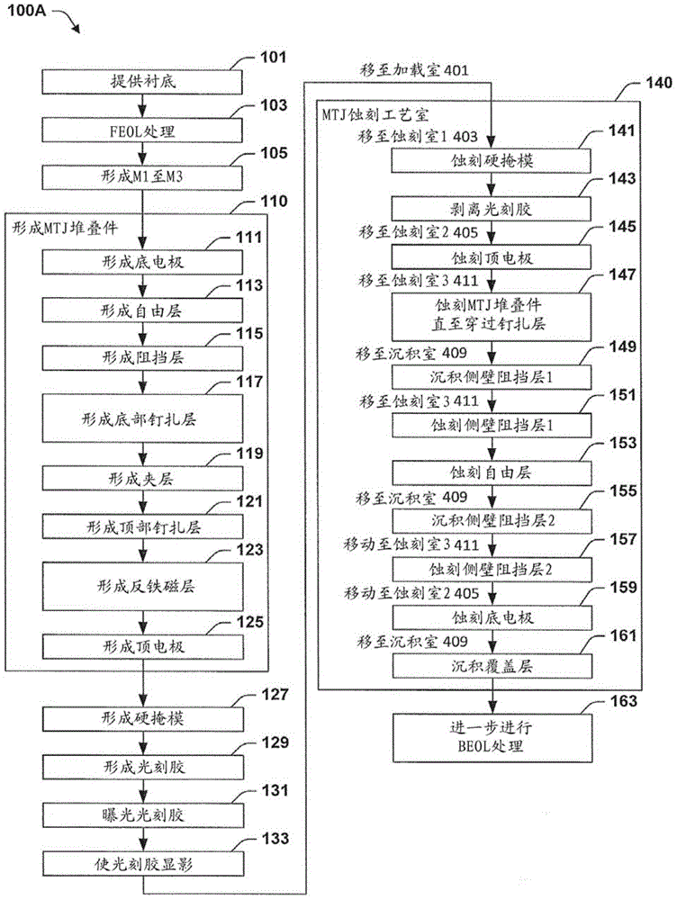
[0035] figure 1 A flow diagram of proc...


PUM


Abstract

An integrated circuit device includes a substrate and a magnetic tunneling junction (MTJ). The MTJ includes at least a pinned layer, a barrier layer, and a free layer. The MTJ is formed over a surface of the substrate. Of the pinned layer, the barrier layer, and the free layer, the free layer is formed first and is closest to the surface. This enables a spacer to be formed over a perimeter region of the free layer prior to etching the free layer. Any damage to the free layer that results from etching or other free layer edge-defining process is kept at a distance from the tunneling junction by the spacer.

Description

technical field [0001] The invention relates to an integrated circuit device with a magnetic tunnel junction and a manufacturing method thereof. Background technique [0002] Magnetic media, such as those used in hard disk drives and magnetic tape, can store information for long periods of time. With traditional magnetic media, data access time is limited by the mechanical system. Both dynamic random access memory (DRAM) and static random access memory (SRAM) have data access times on the order of nanoseconds for read and write operations. These memory types are volatile: only power is supplied to refresh the capacitor charges in DRAM and to keep transistors on in SRAM to store data. The increasing demand for flash memory reflects the need for non-volatile memory. Flash memory technology has relatively low access times (in the μm range) and can only be rewritten a limited number of times. For these reasons, there has been intense interest in commercializing magnetoresist...

Claims


Application Information

Patent Timeline
Patent Type & Authority Applications(China)
IPC IPC(8): H01L43/08H01L27/22
CPCH01L43/08H01L43/02H01L43/12H10N50/80H10N50/10H10N50/01H10N50/85
Inventor 黄韦翰宋福庭徐晨祐刘世昌蔡嘉雄
Owner TAIWAN SEMICON MFG CO LTD
Learn More