ON CELL solid-state full lamination module processing method
A processing method and a fully laminating technology, applied in chemical instruments and methods, optics, lamination devices, etc., can solve the problems of low yield, excessive wiping labor, and easy curing, and achieve high processing yield and processing. Simple process and high assembly precision
- Summary
- Abstract
- Description
- Claims
- Application Information
AI Technical Summary
Problems solved by technology
Method used
Image
Examples
Embodiment Construction
[0021] The following will clearly and completely describe the technical solutions in the embodiments of the present invention with reference to the drawings in the embodiments of the present invention.
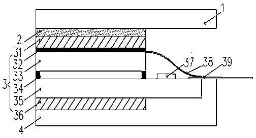
[0022] Such as figure 1 As shown, the structure of an ON CELL solid-state fully laminating module includes a cover glass 1, a solid OCA optical glue 2, an upper polarizer 31, an upper polarizer, and an ITO circuit 32 stacked from top to bottom. CELL TFT liquid crystal display color filter substrate 33, TFT liquid crystal in the middle and frame glue layer 34 around it, ON CELL TFT liquid crystal display lower TFT substrate 35, lower polarizer 36, DRIVER IC37, SENSOR FPC38, TFT FPC39 and backlight 4.
[0023] The embodiment of the present invention provides a kind of ON CELL solid-state full lamination module processing method: After bonding the DRIVER IC (37) at the IC MASK place on the lower TFT substrate (35) of the ON CELL TFT liquid crystal display, the ON CELL TFT liquid ...
PUM
 Abstract
Description
Claims
Application Information
 - R&D
- Intellectual Property
- Life Sciences
- Materials
- Tech Scout
- Unparalleled Data Quality
- Higher Quality Content
- 60% Fewer Hallucinations
Browse by: Latest US Patents, China's latest patents, Technical Efficacy Thesaurus, Application Domain, Technology Topic, Popular Technical Reports.
© 2025 PatSnap. All rights reserved.Legal|Privacy policy|Modern Slavery Act Transparency Statement|Sitemap|About US| Contact US: help@patsnap.com

