CdZnOS quaternary ZnO alloy semiconductor material and preparation method thereof
A semiconductor and alloy technology, applied in the field of semiconductor optoelectronic material preparation, can solve problems such as CdZnOS quaternary ZnO alloy semiconductor materials that have not yet been seen, and achieve the effects of easy control, simple equipment and operation process
- Summary
- Abstract
- Description
- Claims
- Application Information
AI Technical Summary
Problems solved by technology
Method used
Image
Examples
Embodiment 1
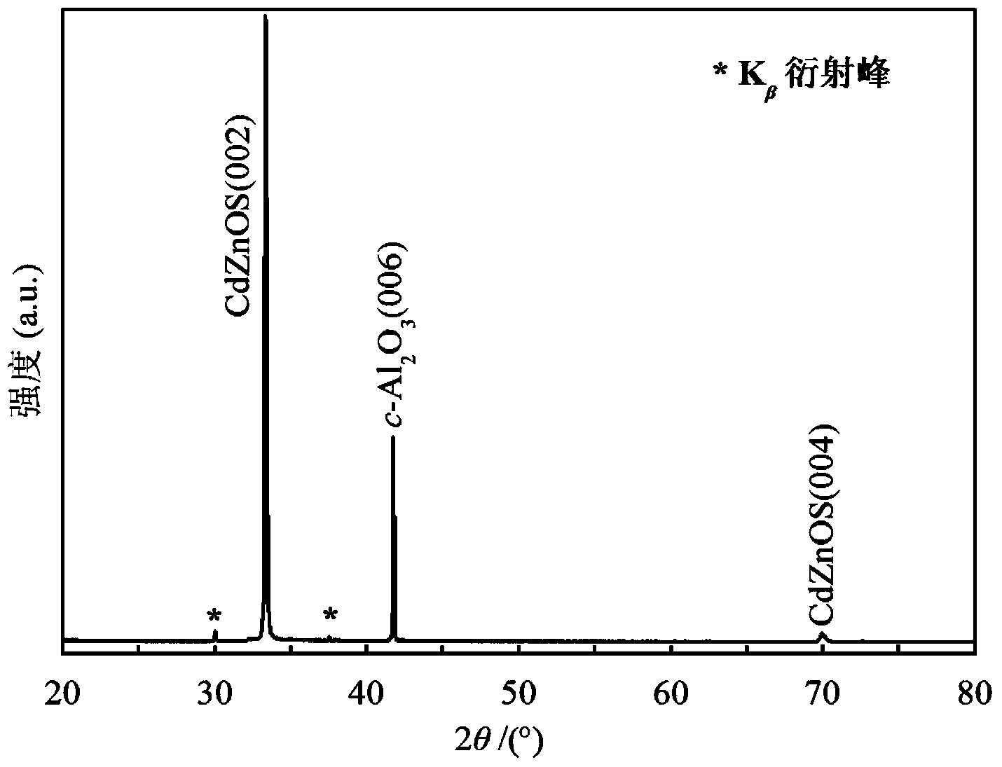
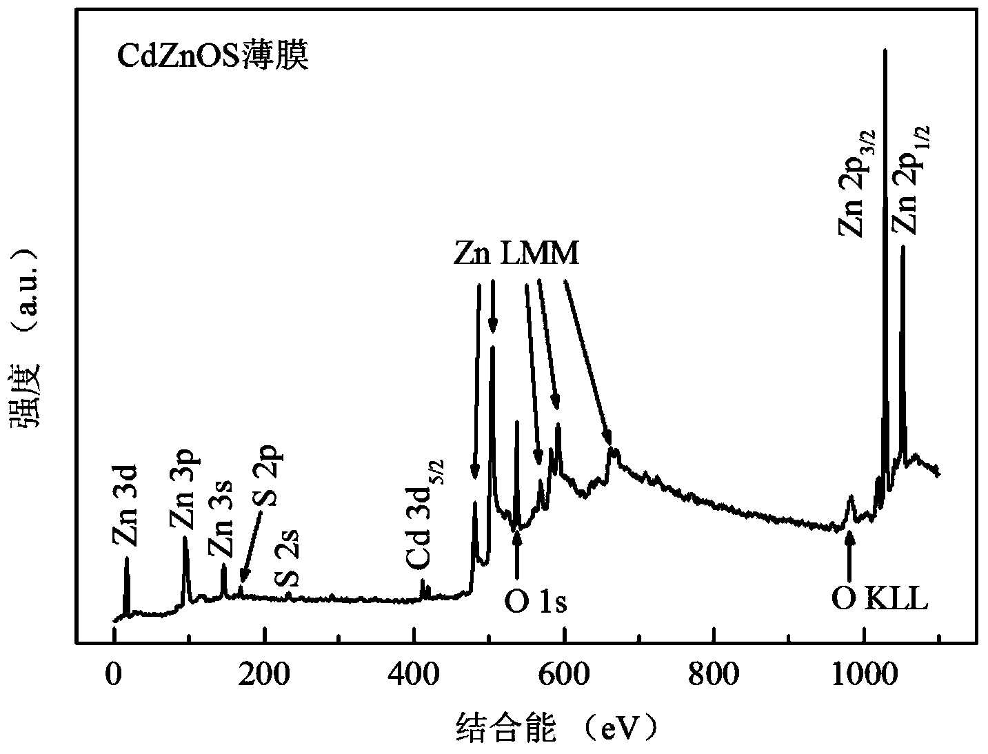
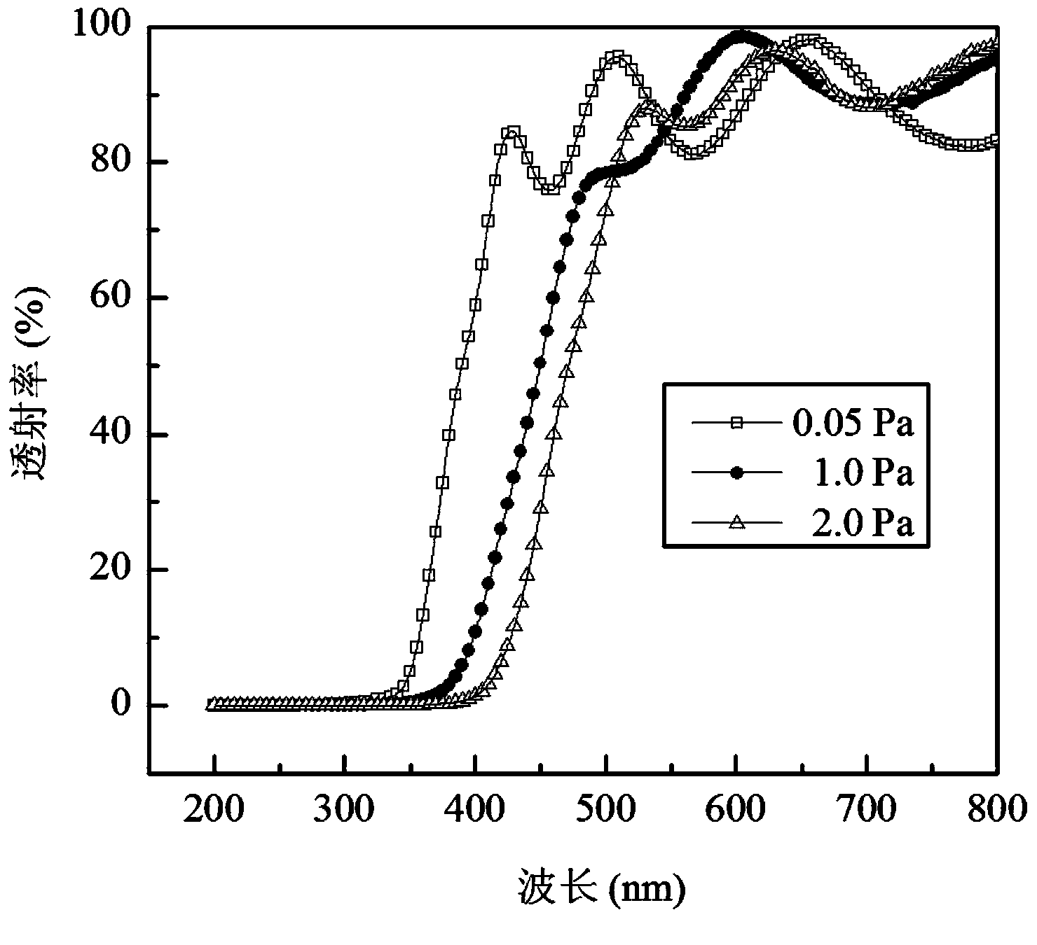
[0028] Weigh 21.8880 g of ZnS powder and 8.1120 g of CdO powder (molar ratio ZnS:CdO=80:20) and place them in a ball mill jar, add 18 mL of deionized water and ball mill for 4 hours, and then dry them in a vacuum oven at 100°C and 0.1Pa 6 hours. The dried powder was added with 1.8 mL of deionized water to fully grind and stir, and then pressed into a circular green sheet with a diameter of 21 mm and a thickness of 2 mm. The billets are placed in a crucible and placed in a vacuum tube furnace, surrounded by powders of the same composition and high-purity sulfur powder. The vacuum tube furnace was evacuated to 0.1 Pa, and then high-purity argon was introduced. Under a protective atmosphere, the temperature of the tube furnace was raised to 600° C. and kept for 3 hours, and then naturally cooled to room temperature to obtain the desired ceramic material. The ceramic material is used as the laser ablation target, and the c-plane sapphire is used as the substrate. The substrate ...
Embodiment 2
[0031] Weigh 21.8880 g of ZnS powder and 8.1120 g of CdO powder (molar ratio ZnS:CdO=80:20) and place them in a ball mill jar, add 18 mL of deionized water and ball mill for 4 hours, and then dry them in a vacuum oven at 100°C and 0.1Pa 6 hours. The dried powder was added with 1.8 mL of deionized water to fully grind and stir, and then pressed into a circular blank with a diameter of 21 mm and a thickness of 3 mm. The green sheet is placed in a crucible and placed in a vacuum tube furnace, and the powder and sulfur powder with the same composition are placed around it. The vacuum tube furnace was evacuated to 0.1 Pa, and then high-purity argon was introduced. Under a protective atmosphere, the temperature of the tube furnace was raised to 600° C. and kept for 3 hours, and then naturally cooled to room temperature to obtain the desired ceramic material. The ceramic material is used as the laser ablation target, and the c-plane sapphire is used as the substrate. The substrate...
Embodiment 3
[0034]Weigh 13.9143 grams of ZnS powder and 1.0857 grams of CdO powder (molar ratio ZnS:CdO=95:5) and place them in a ball mill jar, add 9 mL of deionized water and ball mill for 4 hours, and then dry them in a vacuum oven at 100°C and 0.1Pa 6 hours. The dried powder was added with 0.9 mL of deionized water to fully grind and stir, and then pressed into a circular blank with a diameter of 21 mm and a thickness of 2 mm. The billets are placed in a crucible and placed in a vacuum tube furnace, surrounded by powders of the same composition and high-purity sulfur powder. The vacuum tube furnace was evacuated to 0.1 Pa, and then high-purity argon was introduced. Under a protective atmosphere, the temperature of the tube furnace was raised to 700° C. and kept for 3 hours, and then naturally cooled to room temperature to obtain the desired ceramic material. The ceramic material is used as the laser ablation target, and the c-plane sapphire is used as the substrate. The substrate w...
PUM
| Property | Measurement | Unit |
|---|---|---|
| thickness | aaaaa | aaaaa |
| band gap | aaaaa | aaaaa |
Abstract
Description
Claims
Application Information
 - R&D
- Intellectual Property
- Life Sciences
- Materials
- Tech Scout
- Unparalleled Data Quality
- Higher Quality Content
- 60% Fewer Hallucinations
Browse by: Latest US Patents, China's latest patents, Technical Efficacy Thesaurus, Application Domain, Technology Topic, Popular Technical Reports.
© 2025 PatSnap. All rights reserved.Legal|Privacy policy|Modern Slavery Act Transparency Statement|Sitemap|About US| Contact US: help@patsnap.com


