Phase change memory V-Sb-Te phase change material system and preparing method thereof
A technology of phase change memory and phase change materials, which is applied in the field of V-Sb-Te phase change material system and its preparation, can solve the problems of failure to meet the performance requirements of phase change materials, poor thermal stability of amorphous state, and limited application development, etc. problem, to achieve the best data retention and phase stability, good shrinkable performance, and reduce the effect of volume change rate
- Summary
- Abstract
- Description
- Claims
- Application Information
AI Technical Summary
Problems solved by technology
Method used
Image
Examples
Embodiment 1
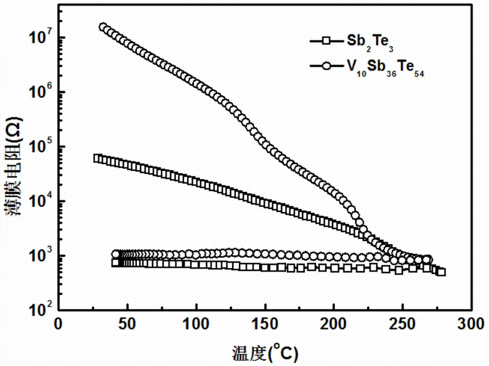
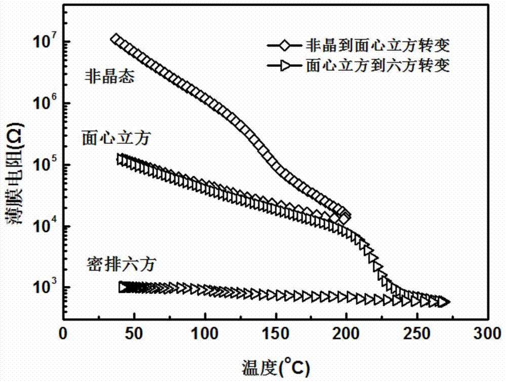
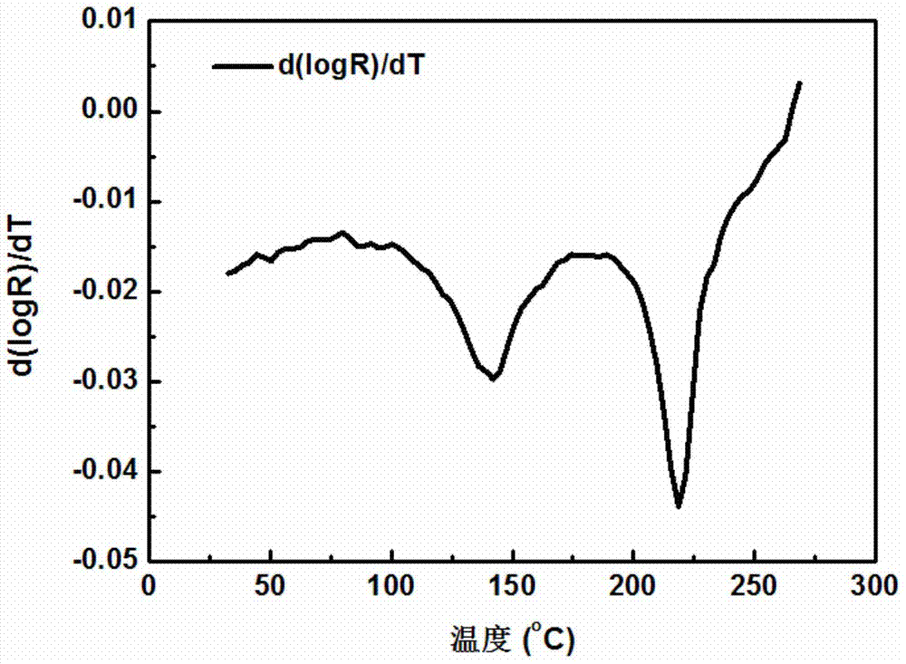
[0023] This embodiment provides a V-Sb-Te phase change material system for phase change memory, wherein the V-Sb-Te phase change material system is formed by doping V on the basis of the Sb-Te phase change material system , whose general chemical formula is V 100-x-y Sb x Te y , wherein, 0.5≤x / y≤4 (where x / y represents the ratio of x to y), and 50≤x+y≤99.99 (where x+y represents the sum of x and y).
[0024] Preferably, at the V 100-x-y Sb x Te y Among them, 1.6≤x / y≤4, wherein, the value range of x is 20≤x≤80, the value range of y is 10≤y≤65, and the atomic percentage of V is not more than 50%. In this embodiment, in the V—Sb—Te phase change material system, the atomic percentage of V is 0.1%˜30%.
[0025] The V-Sb-Te phase-change material system can realize the reversible change of optical reflectivity under the action of laser pulse, and the reversible change of resistivity under the action of electric pulse, so as to realize the function of storing data.
[0026] Thi...
Embodiment 2
[0033] This embodiment provides a V-Sb-Te phase change material for phase change memory, the general chemical formula of the V-Sb-Te phase change material is V 30 Sb 28 Te 42 , and using Sb 2 Te 3 Co-sputtering of alloy target and V elemental target to obtain V 30 Sb 28 Te 42 For thin films, different thicknesses of materials can be controlled by controlling the sputtering time. In this embodiment, sputtering is under 99.999% argon atmosphere, Sb 2 Te 3 The alloy target is sputtered with a DC power supply, and the V target is sputtered with a radio frequency power supply. The sputtering time is 20 minutes, and the obtained V 30 Sb 28 Te 42 The film thickness is about 120nm. where, to obtain V 30 Sb 28 Te 42 Compared with the traditional Sb-Te phase change material, the performance of the thin film is improved in terms of thermal stability and data retention ability.
Embodiment 3
[0035] This embodiment provides a V-Sb-Te phase change material for phase change memory, the general chemical formula of the V-Sb-Te phase change material is V 1 Sb 40 Te 59 , and using Sb 2 Te 3 Co-sputtering of alloy target and V elemental target to obtain V 1 Sb 40 Te 59 For thin films, different thicknesses of materials can be controlled by controlling the sputtering time. In this embodiment, sputtering is under 99.999% argon atmosphere, Sb 2 Te 3 The alloy target is sputtered with a DC power supply, and the V target is sputtered with a radio frequency power supply. The sputtering time is 20 minutes, and the obtained V 1 Sb 40 Te 59 The film thickness is about 120nm. where, to obtain V 1 Sb 40 Te 59 Compared with the traditional Sb-Te phase change material, the performance of the thin film is improved in terms of thermal stability and data retention ability.
PUM
| Property | Measurement | Unit |
|---|---|---|
| thickness | aaaaa | aaaaa |
Abstract
Description
Claims
Application Information
 - Generate Ideas
- Intellectual Property
- Life Sciences
- Materials
- Tech Scout
- Unparalleled Data Quality
- Higher Quality Content
- 60% Fewer Hallucinations
Browse by: Latest US Patents, China's latest patents, Technical Efficacy Thesaurus, Application Domain, Technology Topic, Popular Technical Reports.
© 2025 PatSnap. All rights reserved.Legal|Privacy policy|Modern Slavery Act Transparency Statement|Sitemap|About US| Contact US: help@patsnap.com


