A kind of led tube core with ito nano-column mesh film and preparation method thereof
A technology of nanocolumns and LED epitaxial wafers, which is applied in semiconductor/solid-state device manufacturing, ion implantation plating, coating, etc., and can solve the problem that ITO nanocolumn films cannot be used for current spreading layers
- Summary
- Abstract
- Description
- Claims
- Application Information
AI Technical Summary
Problems solved by technology
Method used
Image
Examples
Embodiment 1
[0039] The LED epitaxial wafer in this embodiment is a GaN epitaxial wafer.
[0040] A preparation method of an LED tube core with an ITO nanocolumn reticular film, comprising the following steps:
[0041] Step 1) Clean the GaN epitaxial wafer. The cleaning method for the LED epitaxial wafer is as follows: boil off the surface grease of the LED epitaxial wafer with acetone, remove the acetone with ethanol or isopropanol, and remove the LED epitaxial wafer with reducing hydrochloric acid or aqua regia. The oxide layer on the surface of the chip, and finally clean and dry the LED epitaxial wafer with deionized water;
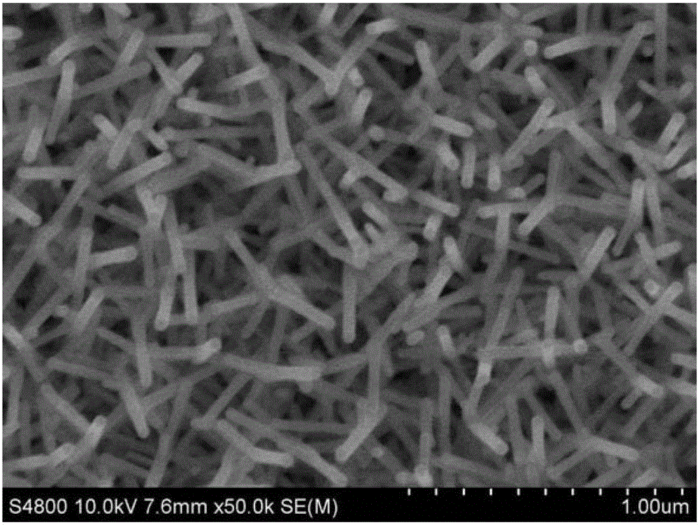
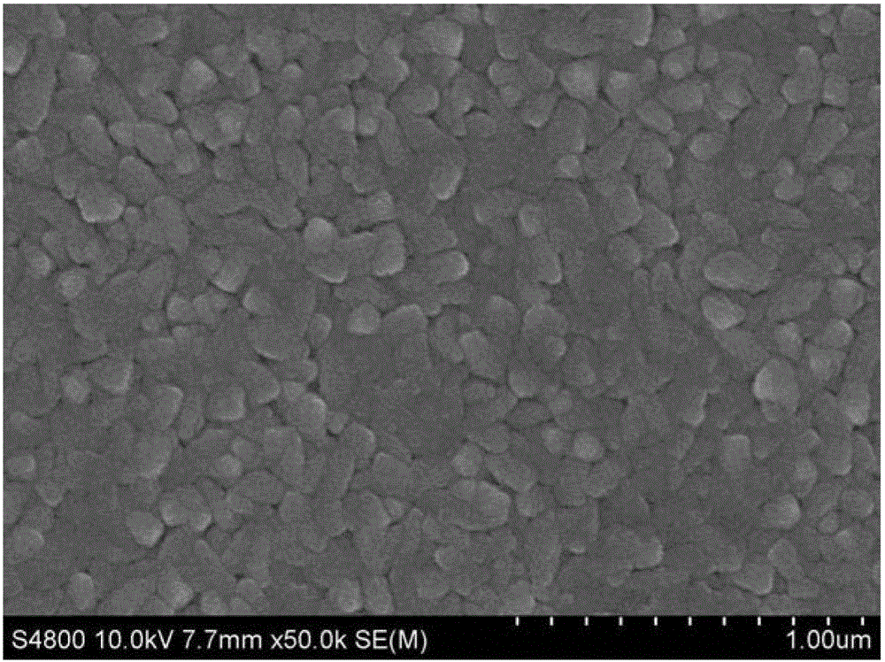
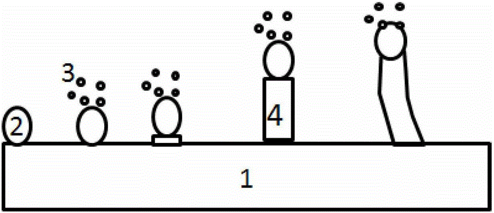
[0042] Step 2) Prepare the ITO nano-column network film on the LED epitaxial wafer after cleaning. The preparation method is to use the VLS crystal growth mechanism to directly evaporate the ITO nano-column network film on the surface of the LED epitaxial wafer under a high-temperature vacuum environment. The high temperature environment refers to the vaporizatio...
Embodiment 2
[0050] Such as Figure 4 shown.
[0051] This embodiment provides an LED die with an ITO nanocolumn network film prepared by the method described in Example 1, including a GaN epitaxial wafer and an ITO nanocolumn network film prepared on the GaN epitaxial wafer. The thickness of the ITO nanocolumn network thin film is 300nm.
Embodiment 3
[0056] Such as Figure 6 shown.
[0057] As described in Example 1, a method for preparing an LED tube core with an ITO nanocolumn reticular film, the difference is that the LED epitaxial wafer is a GaAs quaternary epitaxial wafer of AlGaInP quaternary red-yellow light;
[0058] The step (1) cleaning the GaAs quaternary epitaxial wafer to remove back phosphorus;
[0059] The step (2) uses electron beams to directly evaporate the ITO nano-column network film on the GaAs quaternary epitaxial wafer in a high-temperature vacuum atmosphere, wherein the temperature of the surface of the GaAs quaternary epitaxial wafer is 260 ° C, and the oxygen flow rate is 0 sccm / m 3 , vacuum degree≤3×10 -5 Pa vacuum environment, vapor deposition of ITO nano-column network film 220nm;
[0060] The step (3) prepares an ohmic contact layer on the LED epitaxial wafer treated in the step (2), that is, prepares the P electrode and the N electrode of the LED chip, and finally makes the LED die, and th...
PUM
| Property | Measurement | Unit |
|---|---|---|
| thickness | aaaaa | aaaaa |
| thickness | aaaaa | aaaaa |
| thickness | aaaaa | aaaaa |
Abstract
Description
Claims
Application Information
 - R&D Engineer
- R&D Manager
- IP Professional
- Industry Leading Data Capabilities
- Powerful AI technology
- Patent DNA Extraction
Browse by: Latest US Patents, China's latest patents, Technical Efficacy Thesaurus, Application Domain, Technology Topic, Popular Technical Reports.
© 2024 PatSnap. All rights reserved.Legal|Privacy policy|Modern Slavery Act Transparency Statement|Sitemap|About US| Contact US: help@patsnap.com


