A kind of preparation method of crater-shaped patterned sapphire substrate
A technology for patterning sapphire and sapphire substrates, which is applied to the photolithographic process of the patterned surface, optical mechanical equipment, instruments, etc., and can solve the problems of high cost of imprinting templates and restrictions on the commercial application of nanoimprinting
- Summary
- Abstract
- Description
- Claims
- Application Information
AI Technical Summary
Problems solved by technology
Method used
Image


Examples
Embodiment 1
[0059] In this embodiment, the sapphire substrate is wet-etched, and the hard mask is used as the mask. The method for preparing the crater-type patterned sapphire substrate of this embodiment includes the following steps:
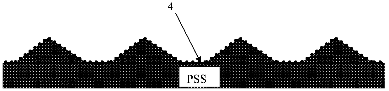
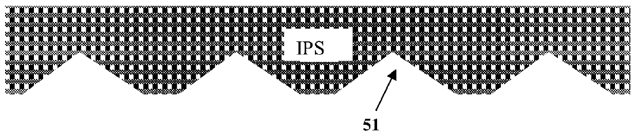
[0060] 1) Surface cleaning and anti-sticking treatment for commercial PSS: the profile of PSS is as figure 1 As shown, the micron PSS pattern 31 on the sapphire substrate is a triangular arrangement of round packets, forming an array of protrusions. The bottom diameter of the round packets is 2 microns, the height is 1.5 microns, and the period is 3 microns; trimethyl fluorosilane is used as the resistance Adhesive, soak the PSS in the anti-adhesive for 1-10 minutes after cleaning, and form a trimethylfluorosilane monomolecular anti-adhesive layer 4 on the surface of the PSS after drying, such as figure 2 As shown, and volatilize excess molecules.
[0061] 2) Use hot embossing to transfer the micron PSS pattern 31 to the intermediate polymer template IPS: Use t...
Embodiment 2
[0069] In this embodiment, the sapphire substrate is dry-etched, and the hard mask is used as the mask. The method for preparing the crater-shaped patterned sapphire substrate of this embodiment includes the following steps:
[0070] 1) Same as Example 1.
[0071] 2) Same as Example 1.
[0072] 3) Use acetone, ethanol and deionized water to clean the surface of the sapphire substrate 1 successively. After cleaning, a layer of hard mask 211 with high selectivity ratio is deposited on the surface of the sapphire substrate, such as Ni, Mo, W, etc. The thickness is 100 nanometers; then, 150-500 nanometers thick nano-imprint glue is spin-coated on the hard mask; for hard masks with poor adhesion, spray on the hard mask before coating the nano-imprint glue Corresponding tackifier; after spin-coating nanoimprint adhesive 210, pre-baked under high temperature conditions at 100°C for 5 minutes.
[0073] 4) Same as Example 1
[0074] 5) Remove the residual glue produced after the nanoimprinting...
Embodiment 3
[0078] In this embodiment, dry etching is used to etch the sapphire substrate, and nanoimprinting glue is used as a mask. The preparation method of the crater-shaped patterned sapphire substrate of this embodiment includes the following steps:
[0079] 1) Because nanoimprinting glue is used as a mask in step 5), and the selection ratio of nanoimprinting glue to sapphire etching is small, the annular protrusions need to be higher than the unimprinted glue layer by more than 1 micron, so It is necessary to select a PSS with a steep side wall of the protrusion, an angle of 60° to 80° with the substrate, and a height of the protrusion of 1.5 to 2 microns as a template, and the others are the same as in the first embodiment.
[0080] 2) Same as Example 1.
[0081] 3) Use acetone, ethanol and deionized water to clean the surface of the sapphire substrate 1. After cleaning, spin-coating a nanoimprinting glue with a high selection ratio as a mask on the sapphire substrate. The thickness of t...
PUM
| Property | Measurement | Unit |
|---|---|---|
| diameter | aaaaa | aaaaa |
| height | aaaaa | aaaaa |
| thickness | aaaaa | aaaaa |
Abstract
Description
Claims
Application Information
 - R&D
- Intellectual Property
- Life Sciences
- Materials
- Tech Scout
- Unparalleled Data Quality
- Higher Quality Content
- 60% Fewer Hallucinations
Browse by: Latest US Patents, China's latest patents, Technical Efficacy Thesaurus, Application Domain, Technology Topic, Popular Technical Reports.
© 2025 PatSnap. All rights reserved.Legal|Privacy policy|Modern Slavery Act Transparency Statement|Sitemap|About US| Contact US: help@patsnap.com