
Method for bonding and splicing seed crystals for monocrystalline silicon ingots and crucible for ingots

A technology similar to single crystal silicon and single crystal silicon, applied in the direction of single crystal growth, single crystal growth, chemical instruments and methods, etc. Fleece effect and conversion efficiency, affecting the quality of monocrystalline silicon ingots, etc., to achieve the effects of fewer defects, preventing the generation of dislocation sources, and low dislocation density

Active Publication Date: 2016-05-25
JIANGXI SAI WEI LDK SOLAR HI TECH CO LTD
View PDF6 Cites 0 Cited by
  • Summary
  • Abstract
  • Description
  • Claims
  • Application Information

AI Technical Summary

Problems solved by technology

[0004] Seed crystals are obtained by mechanical cutting, so there will be damaged layers or crystal dangling bonds on the surface. During the seeding process of quasi-single crystals, the surface defects of seed crystals can easily lead to the generation of dislocations, which will continue to multiply and develop, affecting subsequent crystals. quality;
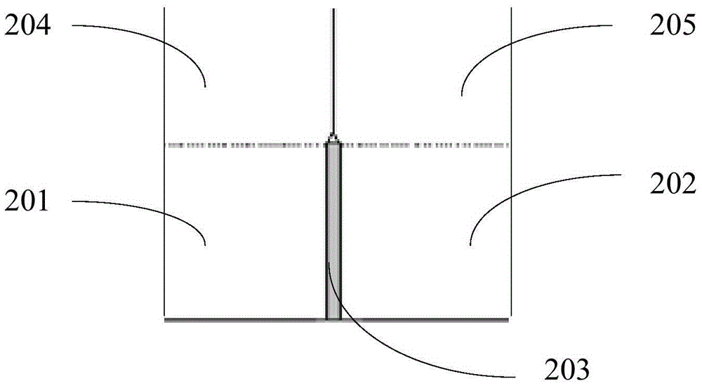
[0005] The seed crystal layer is made of multiple single-crystal seed crystals by physical splicing, so it is difficult to ensure that there are no gaps between the seed crystals and the seed crystals; during the materialization process, the silicon liquid that is first melted on the upper part of the seed crystals will flow down along the gaps , even into the bottom of the seed crystal; and when the silicon liquid flows down in the gap, the cooling rate is relatively fast, so it is easy to generate dislocation defects and polycrystals in the gap; dislocations or polycrystals in these gaps are in the process of seeding It is easy to seed it up, resulting in polycrystalline regions and dislocation defects in the side and seed crystal gaps in the subsequent stage. Polycrystalline and dislocations affect the texturing effect and conversion efficiency of similar monocrystalline silicon wafers, thereby affecting similar The quality of monocrystalline silicon ingot

Method used


Image

  • Method for bonding and splicing seed crystals for monocrystalline silicon ingots and crucible for ingots
  • Method for bonding and splicing seed crystals for monocrystalline silicon ingots and crucible for ingots
  • Method for bonding and splicing seed crystals for monocrystalline silicon ingots and crucible for ingots

Examples


Embodiment

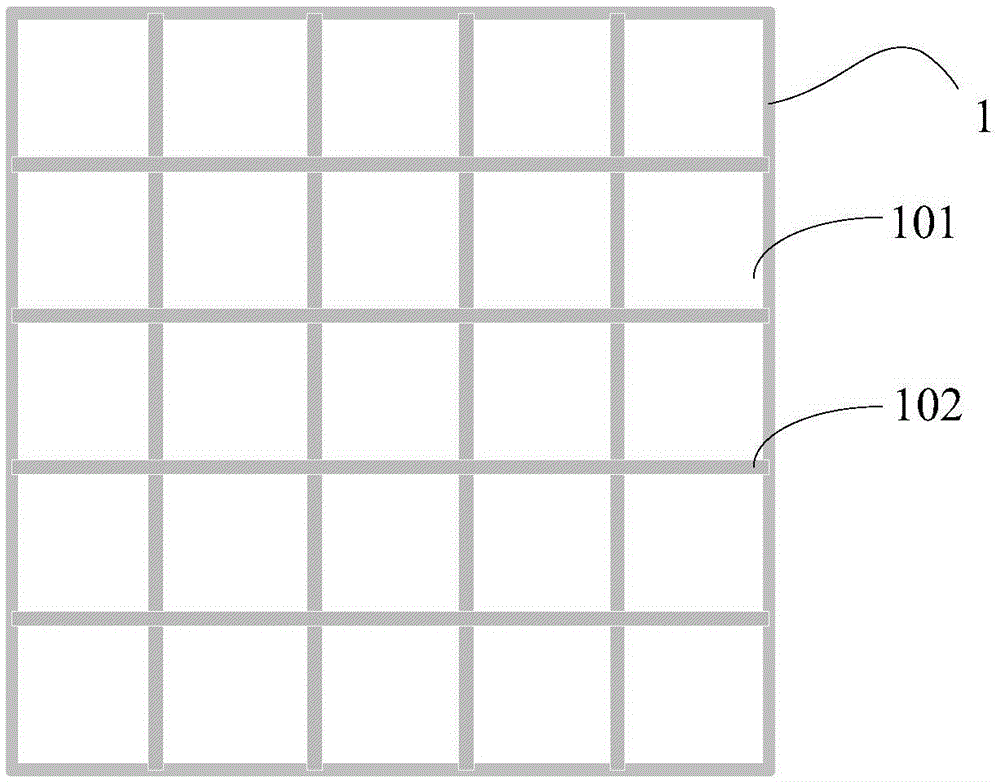
[0049] A method for bonding and splicing seed crystals for quasi-monocrystalline silicon ingots, which is used for directional solidification method quasi-monocrystalline silicon ingots. The specific steps are as follows:

[0050] (1) Cut the seed crystal into a size of 156.8mm×156.8mm, with a thickness of 5mm to 30mm, the size of the seed crystal is not limited to 156.8mm×156.8mm, it can be more or smaller, and the seed crystal preferably has a crystal orientation of (100) Monocrystalline silicon block; after the seed crystal cutting is ready, use an etching method to remove the damaged layer on the surface to be spliced; the silicon etching solution used in the etching method can be an acid etching solution or an alkali etching solution;

[0051] The acid etching solution is a mixed solution of hydrofluoric acid with a mass fraction of 49% and nitric acid with a mass fraction of 63%, and the volume ratio of hydrofluoric acid and nitric acid in the acid etching solution is 1:3...


PUM

PropertyMeasurementUnit
thicknessaaaaaaaaaa

Abstract

The invention provides a bonding and splicing method of seed crystals for monocrystal silicon-like cast ingots. According to the method, an inorganic bonder is adopted for bonding and splicing adjacent seed crystals together to form a seed crystal layer, wherein the inorganic bonder is filled into splicing seams of the seed crystals in the seed crystal layer. When the seed crystal layer is applied to the monocrystal silicon-like cast ingots, defects such as polycrystal and dislocation at seed crystal splicing seams in the ingot casting process can be effectively avoided, the monocrystal silicon-like cast ingots with small defects and high conversion efficiency can be obtained, and the ratio that full-monocrystalline silicon pieces are obtained is greatly improved. The invention further provides a crucible for casting ingots with seed crystal layers. The crucible is applicable to on-scale production of high-quality monocrystal silicon.

Description

technical field [0001] The invention relates to the field of silicon crystal manufacturing, in particular to a method for bonding and splicing seed crystals for quasi-monocrystalline silicon ingots and a crucible for ingots. Background technique [0002] At present, the common manufacturing method of silicon-like single crystal is the directional solidification method. In this method, the seed crystal is laid on the bottom of the flat-bottomed crucible, and the seed crystals are tightly spliced ​​to form a seed crystal layer; then the silicon material is loaded on the seed crystal layer; Through welding control, the molten silicon material is seeded and grown on the seed crystal at the bottom to obtain similar or identical grains to the seed crystal. [0003] Using the above method to grow quasi-single crystals, the main disadvantages include: [0004] Seed crystals are obtained by mechanical cutting, so there will be damaged layers or crystal dangling bonds on the surface....

Claims


Application Information

Patent Timeline
Patent Type & Authority Patents(China)
IPC IPC(8): C30B29/06C30B11/14
Inventor 何亮胡动力雷琦周成张学日
Owner JIANGXI SAI WEI LDK SOLAR HI TECH CO LTD
Learn More