


Quick Research
Generate reliable direction feasibility study reports for your R&D in just a few steps.

Technical Q&A
Discover and master advanced knowledge NOW. Basics, ideas, possibilities, all at once.

Find Solutions
As an expert in R&D theories, this can generate solutions to your technical problems instantly.

Evaluate Feasibility
Analyze your overall solution with one click, know your potential R&D risks in advance.

Monitor Landscape
Get weekly tech updates, stay abreast of the latest tech innovations and key insights.
Polar ingan nanowire material and fabrication method based on m-plane gan
A fabrication method and nanowire technology, applied in the field of microelectronics, can solve the problems of short length, low growth rate and uneven thickness of nanowires, and achieve the effect of increasing growth rate and improving direction consistency.
- Summary
- Abstract
- Description
- Claims
- Application Information
AI Technical Summary
Problems solved by technology
Method used
Image


Examples
Embodiment 1
[0030] Example 1, making a polar InGaN nanowire material with a TiN layer thickness of 15 nm.
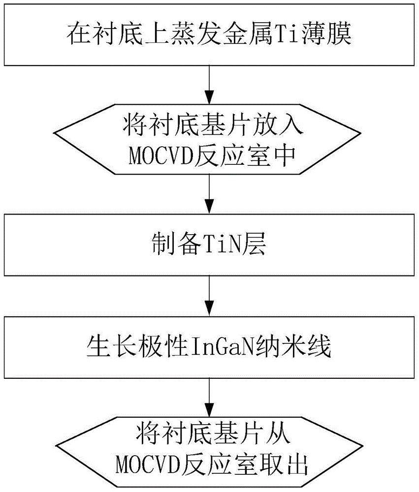
[0031] Step 1, put the m-plane GaN substrate with a thickness of 1000 μm into the electron beam evaporation table E-Beam, in a vacuum of 1.8×10 -3 Under the condition of Pa, evaporate a layer of 15nm Ti metal film at a speed of 0.2nm / s.
[0032] Step 2, place an m-plane GaN substrate with Ti metal in the metal organic chemical vapor deposition MOCVD reaction chamber, heat the reaction chamber after evacuating to make the temperature reach 1200 ° C, under the condition that the reaction chamber pressure is 760 Torr, simultaneously The flow rate of hydrogen and ammonia gas in the reaction chamber is both 10000 sccm for 60 minutes, so that most of the metal Ti reacts with ammonia gas, and a TiN layer with a thickness of 15 nm is formed on the m-plane GaN substrate, and a small part of it does not react with ammonia gas. The reacted metal Ti is randomly distributed on the surface of th...
Embodiment 2
[0035] Example 2, making a polar InGaN nanowire material with a TiN layer thickness of 2 nm.
[0036] Step A, put the m-plane GaN substrate with a thickness of 5 μm into the electron beam evaporation table E-Beam to evaporate a layer of 8nm Ti metal film, and the process conditions are: the vacuum degree is 1.8×10 -3 Pa, the evaporation rate is 0.2nm / s;
[0037] Step B, placing the m-plane GaN substrate with Ti metal in the MOCVD reaction chamber, setting the pressure and heating temperature of the reaction chamber after vacuuming, and then feeding hydrogen and ammonia into the reaction chamber at the same time for a period of time, so that most of the Metal Ti reacts with ammonia gas to form a TiN layer with a thickness of 2nm on the m-plane GaN substrate, and a small part of metal Ti that has not reacted with ammonia gas is randomly distributed on the surface of the TiN layer. The process conditions are: The pressure is 20 Torr, the flow rates of hydrogen and ammonia are bo...
Embodiment 3
[0040] Example 3, preparing a polar InGaN nanowire material with a TiN layer thickness of 8 nm.
[0041] In the first step, a metal Ti film is evaporated.
[0042] The m-plane GaN substrate with a thickness of 1 μm was placed in the E-Beam of the electron beam evaporation station, and the vacuum degree was 1.8×10 -3 Under the condition of Pa, a layer of 2nm Ti metal film was evaporated at a speed of 0.2nm / s.
[0043] The second step is to prepare a TiN layer.
[0044] Put the m-plane GaN substrate with Ti metal in the MOCVD reaction chamber, set the pressure in the reaction chamber to 40Torr after vacuuming, and set the heating temperature to 900°C, and then feed hydrogen gas with a flow rate of 2000sccm and ammonia with a flow rate of 3000sccm into the reaction chamber gas for 8 minutes, so that most of the metal Ti reacts with ammonia gas to form a TiN layer with a thickness of 8nm on the m-plane GaN substrate, and a small part of residual metal Ti that has not reacted wit...
PUM
| Property | Measurement | Unit |
|---|---|---|
| thickness | aaaaa | aaaaa |
| thickness | aaaaa | aaaaa |
| thickness | aaaaa | aaaaa |
Abstract
Description
Claims
Application Information
 - R&D Engineer
- R&D Manager
- IP Professional
- Industry Leading Data Capabilities
- Powerful AI technology
- Patent DNA Extraction
Browse by: Latest US Patents, China's latest patents, Technical Efficacy Thesaurus, Application Domain, Technology Topic, Popular Technical Reports.
© 2024 PatSnap. All rights reserved.Legal|Privacy policy|Modern Slavery Act Transparency Statement|Sitemap|About US| Contact US: help@patsnap.com