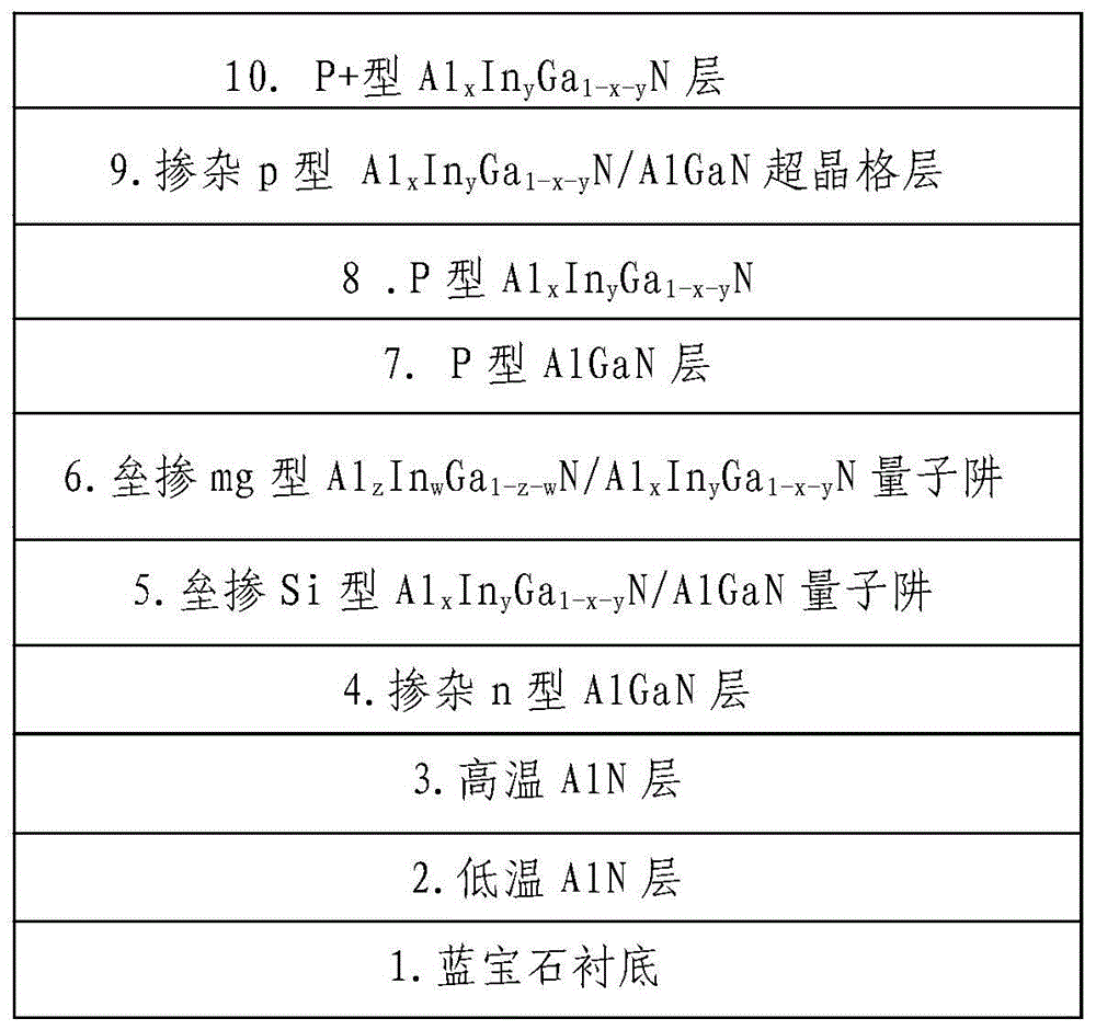
A kind of epitaxial growth method of high-efficiency ultraviolet LED
A technology of epitaxial growth and high light efficiency, applied in electrical components, circuits, semiconductor devices, etc., can solve the problems of high preparation cost, difficulty, and difficulty in p-layer doping, and achieve the effect of increasing radiation power and reducing the difficulty of growth.
- Summary
- Abstract
- Description
- Claims
- Application Information
AI Technical Summary
Problems solved by technology
Method used
Image
Examples
Embodiment 1
[0053] 1. After cleaning the sapphire substrate, put it into the MOCVD equipment and bake it at 1100°C for 10 minutes.
[0054] 2. A low-temperature AlN layer with a thickness of 10 nm is grown at a temperature of 600° C., and the growth pressure is 200 torr.
[0055] 3. Raise the temperature to 1070°C to grow an intrinsic AlN layer with a thickness of 300nm, and the growth pressure is 200torr.
[0056] 4. A layer of 10-period AlN / AlGaN superlattice is grown at a temperature of 1050° C. and 200 torr, with a total thickness of 70 nm.
[0057] 5. Grow a silane-doped n-type AlGaN layer at a temperature of 1050°C with a thickness of 500nm and a pressure of 200torr.
[0058] 6. Grow a 3nm AlxInyGa1-x-yN layer at 850°C in a nitrogen atmosphere of 50torr; then raise the temperature to 950°C and 200torr to grow a 12nm AlGaN layer, doping a small amount of silane during the growth process; then repeat the growth of 3 cycle.
[0059] 7. Then grow a layer of about 3nm Al in nitrogen a...
Embodiment 2
[0068] 1. After cleaning the sapphire substrate, put it into the MOCVD equipment and bake it at 1100°C for 10 minutes.
[0069] 2. A low-temperature AlN layer with a thickness of 10 nm is grown at a temperature of 600° C., and the growth pressure is 200 torr.
[0070] 3. Raise the temperature to 1070°C to grow an intrinsic AlN layer with a thickness of 300nm, and the growth pressure is 200torr.
[0071] 4. Grow a silane-doped n-type AlGaN layer with a thickness of 500nm at a temperature of 1050°C and a pressure of 200torr.
[0072] 5. Grow a layer of about 3nm Al in nitrogen atmosphere 50torr, 850℃ x In y Ga 1-x-y N layer; then raise the temperature to 950°C and 200torr, and then grow a 12nm AlGaN layer, doped with a small amount of silane during the growth process; then repeat the growth for 3 cycles.
[0073] 6. Then grow a layer of about 3nm Al in nitrogen atmosphere 50torr, 850℃ x In y Ga 1-x-y N layer, followed by a layer of Al z In w Ga 1-z-w N(x<z<1, w<y<1, 0<...
Embodiment 3
[0082] 1. After cleaning the sapphire substrate, put it into the MOCVD equipment and bake it at 1100°C for 10 minutes.
[0083] 2. A low-temperature AlN layer with a thickness of 10 nm is grown at a temperature of 600° C., and the growth pressure is 200 torr.
[0084] 3. Raise the temperature to 1070°C to grow an intrinsic AlN layer with a thickness of 300nm, and the growth pressure is 200torr.
[0085] 4. A layer of 10-period AlN / AlGaN superlattice is grown at a temperature of 1050° C. and 200 torr, with a total thickness of 70 nm.
[0086] 5. Grow a silane-doped n-type AlGaN layer with a thickness of 500nm at a temperature of 1050°C and a pressure of 200torr.
[0087] 6. Grow a layer of about 3nm Al in a nitrogen atmosphere of 50torr and 850℃ x In y Ga 1-x-y N layer; then raise the temperature to 950°C and 200torr, and then grow a 12nm AlGaN layer, doped with a small amount of silane during the growth process; then repeat the growth for 3 cycles.
[0088] 7. Then grow a...
PUM
 Abstract
Description
Claims
Application Information
 - R&D
- Intellectual Property
- Life Sciences
- Materials
- Tech Scout
- Unparalleled Data Quality
- Higher Quality Content
- 60% Fewer Hallucinations
Browse by: Latest US Patents, China's latest patents, Technical Efficacy Thesaurus, Application Domain, Technology Topic, Popular Technical Reports.
© 2025 PatSnap. All rights reserved.Legal|Privacy policy|Modern Slavery Act Transparency Statement|Sitemap|About US| Contact US: help@patsnap.com


