Layout structure and method for reducing peak electric field of ldmos device

A device and electric field technology, which is applied in the field of layout structure to reduce the peak electric field of LDMOS devices, can solve problems such as unfavorable device reliability, device failure, and easy breakdown, so as to improve the layout, increase the withstand voltage level, and reduce the electric field intensity. Effect

Active Publication Date: 2016-12-21
SHANGHAI HUAHONG GRACE SEMICON MFG CORP
View PDF6 Cites 0 Cited by
  • Summary
  • Abstract
  • Description
  • Claims
  • Application Information

AI Technical Summary

Problems solved by technology

[0004] In the prior art, the electric field at the bird's beak boundary of the field oxide layer 7 near the source is relatively concentrated, which is prone to breakdown, resulting in device failure
Moreover, this place is the boundary between the field oxygen and the gate oxide, and the electric field is strong. When a voltage is applied to the source end, the hot carrier effect (Hot carrier Effect, HCE) of the device will be increased, which is not conducive to the reliability of the device.

Method used


Image

  • Layout structure and method for reducing peak electric field of ldmos device
  • Layout structure and method for reducing peak electric field of ldmos device
  • Layout structure and method for reducing peak electric field of ldmos device

Examples


Embodiment Construction

[0021] The present invention will be further described in detail below in conjunction with the accompanying drawings and specific embodiments.

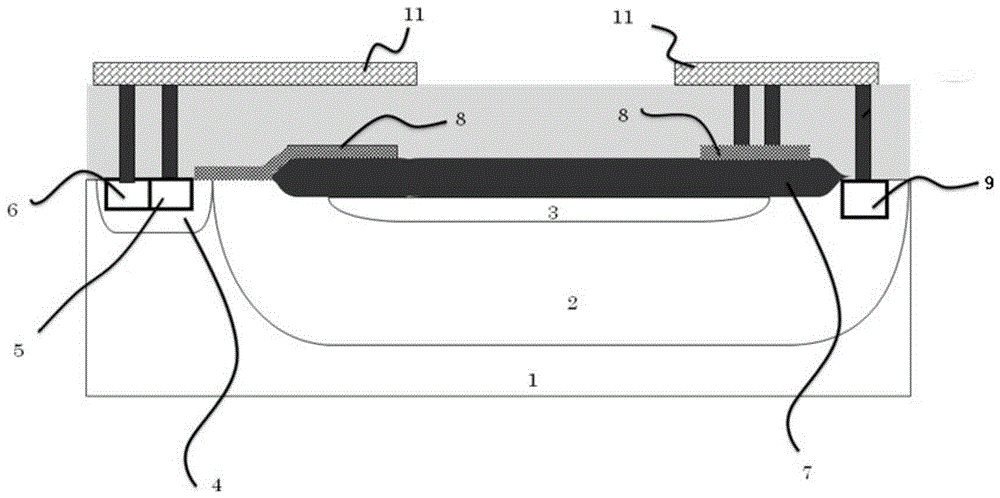
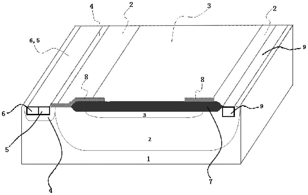
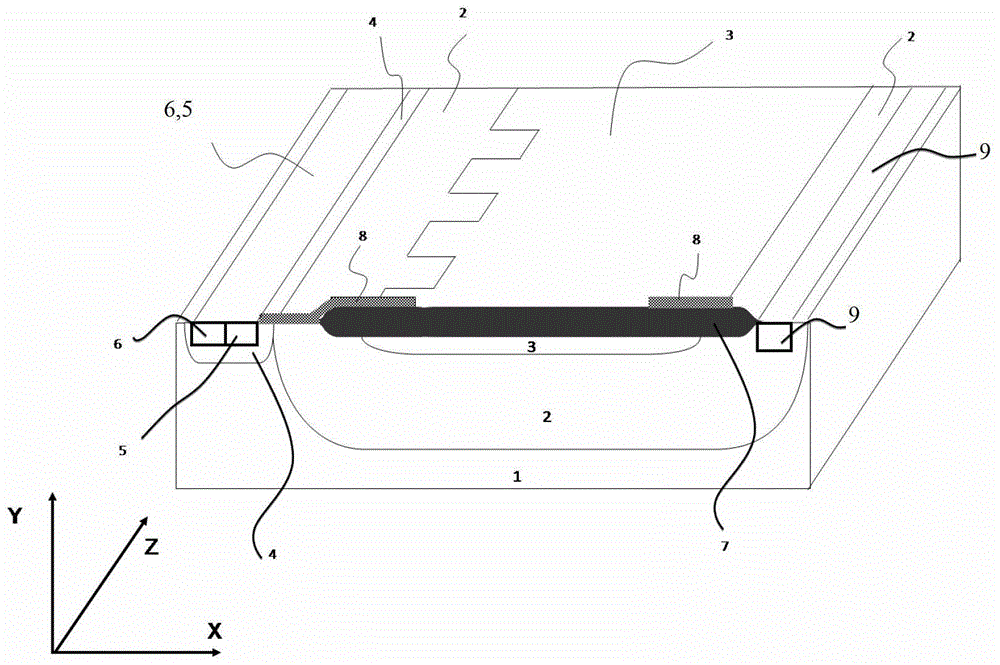
[0022] The method for reducing the peak electric field of an LDMOS device provided by the present invention, the LDMOS device includes a silicon substrate with a first conductivity type, and a deep well with a second conductivity type opposite to the first conductivity type is formed on the silicon substrate, so that The deep well constitutes a drift region; a field oxide layer is formed in the deep well, and a buried layer with the first conductivity type is formed under the field oxide layer, and the buried layer is located on the top or inside of the deep well; the source region of the LDMOS device is composed of The first doped region with the second conductivity type is formed in the well region with the first conductivity type, the well region is located on one side of the field oxide layer, and the drain terminal is composed of ...


PUM


Abstract

The invention discloses a layout structure and method for reducing the peak electric field of an LDMOS device. The LDMOS device includes a silicon substrate of a first conductivity type, and a silicon substrate of a second conductivity type opposite to the first conductivity type is formed on the silicon substrate. Deep well; a field oxide layer is formed in the deep well, and a buried layer of the first conductivity type is formed under the field oxide layer, and the buried layer is located on the top or inside of the deep well; the source region of the LDMOS device is doped by the first conductivity type region, the first doped region is formed in the well region of the first conductivity type, the drain end is composed of the second doped region of the second conductivity type, the second doped region is formed in the deep well, and the buried Layers alternate with deep wells at least on the side close to the source region. The buried layer and deep wells of the present invention are interlaced to form several PN junctions, and the PN junctions generate a self-built electric field, which weakens the electric field generated by the drain terminal voltage, reduces the electric field intensity at the bird's beak near the source end, and improves The withstand voltage level of the device.

Description

technical field [0001] The invention relates to a semiconductor device structure, in particular to a layout structure and method for reducing the peak electric field of an LDMOS device. Background technique [0002] With the awareness of energy conservation and emission reduction gradually becoming popular among the people, and the development of smart grid projects, the market prospect of power semiconductors (Power Integrated Circuit, PIC for short), especially ultra-high voltage power semiconductors in the field of power consumption and distribution, will be very broad, such as the LED market. Electric lighting, high-efficiency motor drive, transformation of distribution network, AC / DC conversion of electric energy, etc. Among all power semiconductor devices, LDMOS (Lateral Double Diffused MOSFET, that is, lateral double diffused metal oxide semiconductor field effect transistor) high-voltage devices have the characteristics of high operating voltage, relatively simple pr...

Claims


Application Information

Patent Timeline
Patent Type & Authority Patents(China)
IPC IPC(8): H01L29/78H01L29/06H01L21/336
CPCH01L29/0619H01L29/7816H01L29/0634H01L29/0692H01L29/404H01L29/42368H01L29/7835
Inventor 宁开明
Owner SHANGHAI HUAHONG GRACE SEMICON MFG CORP
Why Eureka
Try Eureka