Cuprous oxide nanowire porous film as well as preparation method and application thereof
A technology of porous film and cuprous oxide, which is applied in the field of nanomaterials and photoelectric functional materials
- Summary
- Abstract
- Description
- Claims
- Application Information
AI Technical Summary
Problems solved by technology
Method used
Image

Examples
Embodiment 1
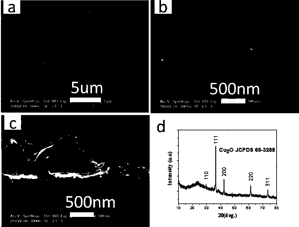
[0024] Deposit a copper film with a thickness of about 100 nanometers on the surface of the glass slide, and then immerse the copper film in an ammonium thiocyanate solution with a concentration of 1 mmol / L. After soaking for 2 hours, sulfur can be formed on the surface of the glass slide. The cuprous cyanate film is fully washed with deionized water, and then the cuprous thiocyanate film is immersed in a sodium hydroxide solution with a concentration of 10 mmol / L for 1 hour, and then the film is taken out from the solution and washed with deionized water. After fully washing and then drying, the cuprous oxide nanowire porous film can be formed in situ on the surface of the glass slide.
[0025] figure 1 (a) and figure 1 (b) is the SEM image of the cuprous oxide film at different magnifications, showing that the cuprous oxide nanowires are randomly stacked to form a interwoven film throughout. figure 1 (c) is a side SEM image of the cuprous oxide film, showing that most n...
Embodiment 2
[0028] Deposit a copper film with a thickness of about 50 nanometers on the surface of the glass slide, and then immerse the copper film in an ammonium thiocyanate solution with a concentration of 1 mmol / L. After soaking for 2 hours, sulfur can be formed on the surface of the glass slide. The cuprous cyanate film is fully washed with deionized water, and then the cuprous thiocyanate film is immersed in a sodium hydroxide solution with a concentration of 10 mmol / L for 1 hour, and then the film is taken out from the solution and washed with deionized water. After fully washing and then drying, the cuprous oxide nanowire porous film can be formed in situ on the surface of the glass slide.
[0029] The results of surface morphology and structural analysis are similar to those of Example 1.
Embodiment 3
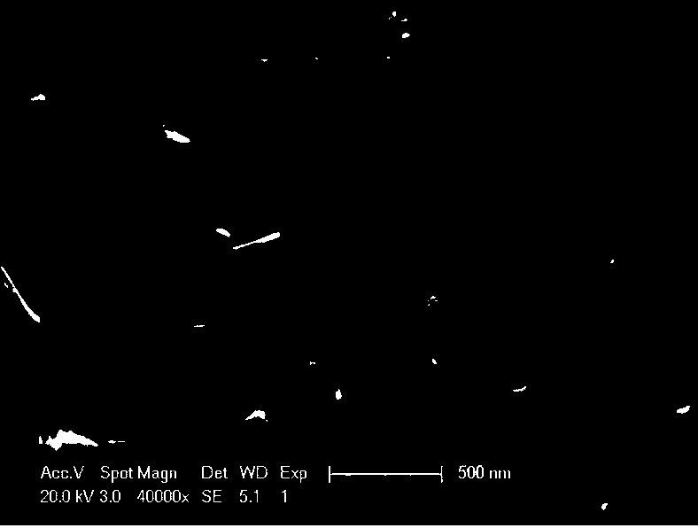
[0031] Deposit a copper film with a thickness of about 150 nanometers on the surface of a flexible PET plastic substrate, then immerse the copper film in an ammonium thiocyanate solution with a concentration of 1 mmol / L, soak for 5 hours, and then it can be deposited on the surface of a glass slide. Form a cuprous thiocyanate film, fully wash with deionized water, and then immerse the cuprous thiocyanate film into a sodium hydroxide solution with a concentration of 10 mmol / L to react for 3 hours, then take out the film from the solution, and use The ion water is fully washed, and then dried, and the cuprous oxide nanowire porous film can be formed in situ on the surface of the PET plastic substrate.
[0032] The cuprous oxide nanowire porous film deposited on the surface of the PET plastic substrate can be bent many times without obvious change.
[0033] A typical SEM image such as image 3 Shown, similar to the result in Example 1.
[0034] The thickness of the cuprous oxide ...
PUM
| Property | Measurement | Unit |
|---|---|---|
| thickness | aaaaa | aaaaa |
| thickness | aaaaa | aaaaa |
| thickness | aaaaa | aaaaa |
Abstract
Description
Claims
Application Information
 - R&D
- Intellectual Property
- Life Sciences
- Materials
- Tech Scout
- Unparalleled Data Quality
- Higher Quality Content
- 60% Fewer Hallucinations
Browse by: Latest US Patents, China's latest patents, Technical Efficacy Thesaurus, Application Domain, Technology Topic, Popular Technical Reports.
© 2025 PatSnap. All rights reserved.Legal|Privacy policy|Modern Slavery Act Transparency Statement|Sitemap|About US| Contact US: help@patsnap.com