Double-diffraction-level Offner imaging spectrometer
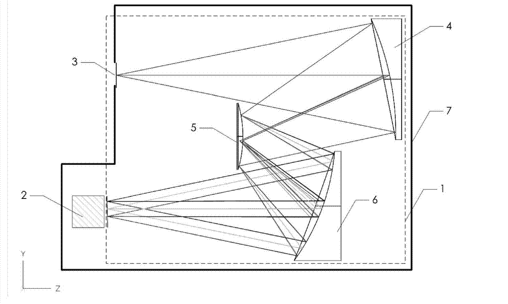
An imaging spectrometer and diffraction order technology, applied in the field of hyperspectral imaging, can solve the problem of increasing the difficulty of correcting off-axis aberration in the spectral dimension direction, improve energy utilization and stray light suppression capability, reduce volume and weight, and reduce weak The effect of polarization sensitivity
- Summary
- Abstract
- Description
- Claims
- Application Information
AI Technical Summary
Problems solved by technology
Method used
Image
Examples
Embodiment 1
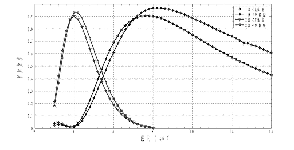
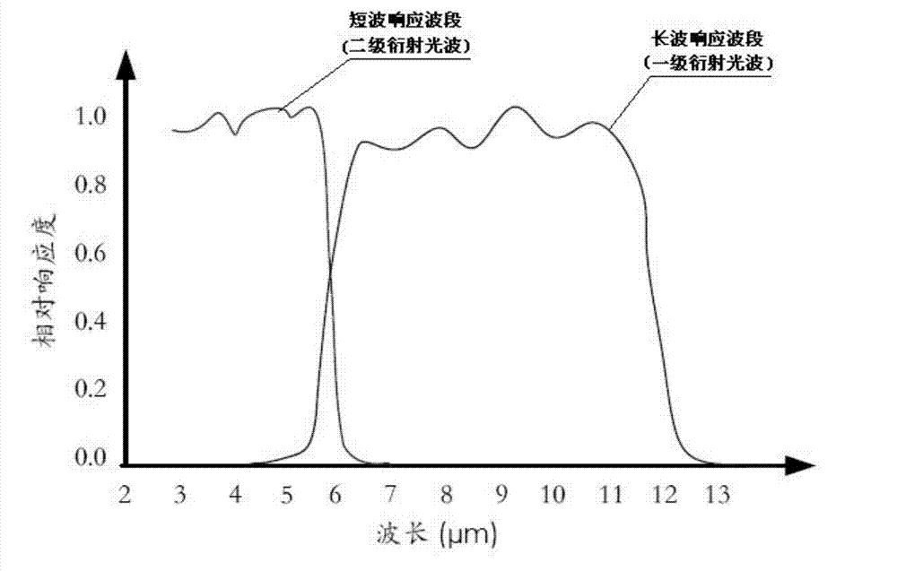
[0013] Example 1: MWIR / LWIR double diffraction order Offner imaging spectrometer
[0014] The first-order and second-order diffraction working wavelength ranges of MWIR / LWIR dual-diffraction-order Offner imaging spectrometers are respectively selected as two octave intervals of 6-12 μm and 3-6 μm, and 6 μm is the connection and transition wavelength value of the two diffraction orders, defined For overlapping wavelengths; the dual-band area array photodetector is a cooled HgCdTe dual-band infrared focal plane array, with 320×256 pixels, 30μm pixel spacing, and response wavelength ranges of 3-6μm and 6-12μm, respectively. The dual-band area array photodetector can be a coaxial laminated sub-band response structure or a planar interlaced sub-band response structure. The coaxial laminated sub-band response structure is composed of photosensitive elements that respond to two different wavebands vertically superimposed and integrated on the detection chip. The two response waveband...
Embodiment 2
[0016] Example 2: VNIR / SWIR Dual Diffraction Order Offner Imaging Spectrometer
[0017]The first-order and second-order diffraction working wavelength ranges of the VNIR / SWIR dual-diffraction order Offner imaging spectrometer are respectively selected from two sections of 1000-2500nm and 500-1000nm, and the overlapping wavelength is 1000nm; this band imaging spectrometer is based on aviation or aerospace platforms. It has important application value in the field of remote sensing detection. The dual-band area array photodetector uses a wide-band HgCdTe monochromatic area array detector, and forms a planar interlaced sub-band response structure by interlacing with two band-pass filter films with different response bands. Broad-band HgCdTe type monochromatic area array detector responds to a wavelength range of 500-2500nm (greater than this range is also acceptable); it has 640×480 pixels and a pixel pitch of 27μm; the low pixel dimension of the detector is used for spatial dire...
PUM
 Abstract
Description
Claims
Application Information
 - R&D
- Intellectual Property
- Life Sciences
- Materials
- Tech Scout
- Unparalleled Data Quality
- Higher Quality Content
- 60% Fewer Hallucinations
Browse by: Latest US Patents, China's latest patents, Technical Efficacy Thesaurus, Application Domain, Technology Topic, Popular Technical Reports.
© 2025 PatSnap. All rights reserved.Legal|Privacy policy|Modern Slavery Act Transparency Statement|Sitemap|About US| Contact US: help@patsnap.com


