A transistor, a pixel unit, an array substrate and a display device

A technology for array substrates and transistors, which is applied in the fields of array substrates and display devices, pixel units, and transistors, and can solve problems such as thin photoresist thickness, affecting TFT performance, and changing TFT width-to-length ratio

Active Publication Date: 2016-01-27
BOE TECH GRP CO LTD +1
View PDF3 Cites 0 Cited by
  • Summary
  • Abstract
  • Description
  • Claims
  • Application Information

AI Technical Summary

Problems solved by technology

[0003] After forming various layers of patterns on the glass substrate, apply photoresist, then perform exposure and development, and then remove the exposed doped semiconductor layer by wet etching and other etching methods to expose the semiconductor layer and form a TFT channel, but The existing processing technology will cause the thickness of the photoresist at the bend of the TFT channel to be thin, resulting in an open circuit at the bend of the TFT channel after exposure and development.
Since an open circuit occurs at the bend of the TFT channel, it will change the width-to-length ratio of the TFT, thereby affecting the performance of the TFT

Method used


Image

  • A transistor, a pixel unit, an array substrate and a display device
  • A transistor, a pixel unit, an array substrate and a display device
  • A transistor, a pixel unit, an array substrate and a display device

Examples


Embodiment Construction

[0027] The specific implementation manners of the present invention will be further described in detail below in conjunction with the accompanying drawings and embodiments. The following examples are used to illustrate the present invention, but are not intended to limit the scope of the present invention.

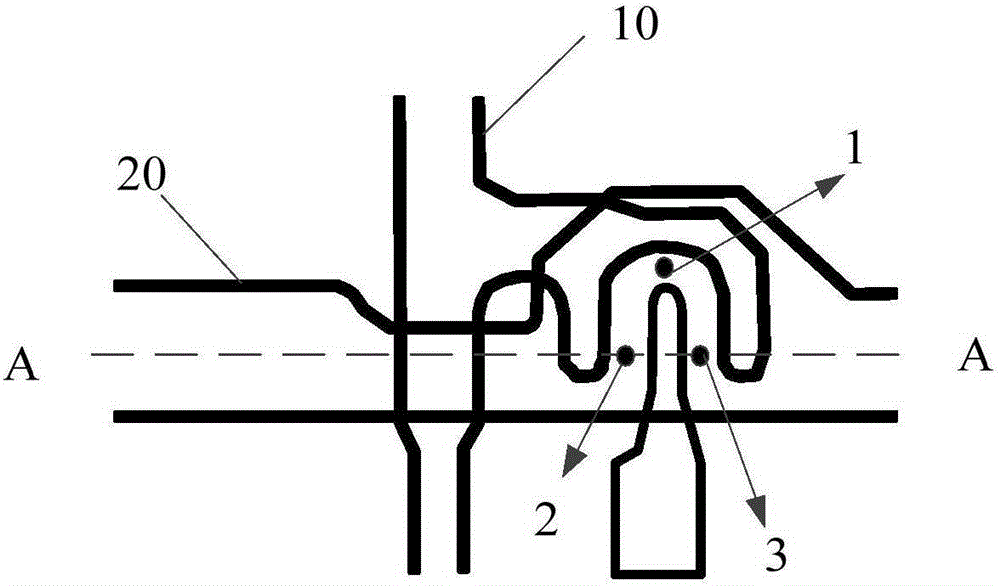
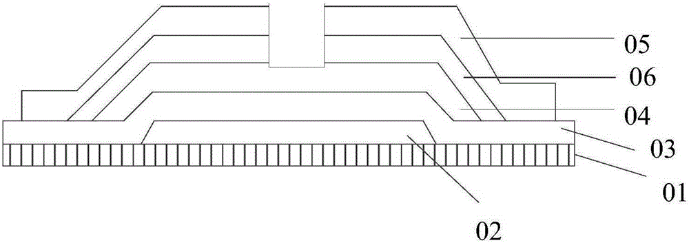
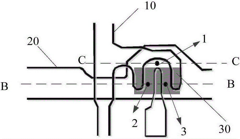
[0028] At present, in the TFT manufacturing process, a gate metal thin film is deposited on a substrate, and a gate electrode and a gate line are obtained through exposure and etching. The gate metal film is generally composed of multi-layer metal films. A specific mask is used to perform exposure and etching processes to form gate electrodes and gate line patterns on the substrate. The gate lines are formed in the pixel area along the horizontal direction.

[0029] Using the same manufacturing process, a gate insulating layer, an active layer, and a source-drain electrode layer are sequentially formed on the gate electrode. After coating the photoresist, the source-drain ...


PUM


Abstract

The invention discloses a thin film transistor. The thin film transistor comprises a grid electrode, a grid insulating layer, an active layer and a source and drain electrode layer; in addition, the thin film transistor further comprises a correction electrode layer which is arranged at the bottom of the grid electrode. The correction electrode layer is deposited in advance before a grid electrode metal layer is formed at the bottom of the grid electrode, the correction electrode layer which is a gasket structure layer is added, and therefore it can be guaranteed that after photoresists are coated and before the photoresists are exposed, the surfaces of the photoresists are planes, a difference value of the thickness of the photoresist of a non-thin film transistor channel bend and the thickness of the photoresist of a thin film transistor channel bend reduces the thickness of a transparent electrode after exposure and development are conducted, the thickness difference of the non-thin film transistor channel bend and the thin film transistor channel bend is reduced, the phenomenon that the photoresist at the thin film transistor channel bend is too thin is avoided, uniformity of the thicknesses of all the photoresists in channels is guaranteed, and the circuit opening probability of the thin film transistor channel bend is reduced. Meanwhile, the invention further provides a pixel unit and an array substrate based on the thin film transistor, and provides a display device based on the array substrate.

Description

technical field [0001] The invention relates to the field of display panel manufacturing, in particular to a transistor, a pixel unit, an array substrate and a display device. Background technique [0002] At present, with the continuous improvement of application requirements, more and more fields use large-size TFT-LCD (ThinFilmTransistor-LiquidCrystalDisplay, thin film field effect transistor liquid crystal display) to achieve display, TFT is produced on the glass substrate, and then based on The above TFTs are made into various layers of graphics, and finally a TFT substrate is obtained. On the TFT substrate, the TFT mainly realizes the switching function, and each liquid crystal pixel on the liquid crystal display is driven and controlled by a thin film transistor TFT. The quality of the TFT processing technology is critical, because the processing technology will affect its performance, and the TFT performance will further have an important impact on the display effect...

Claims


Application Information

Patent Timeline
Patent Type & Authority Patents(China)
IPC IPC(8): H01L29/786H01L27/12
CPCH01L27/1214H01L29/42384H01L29/66007H01L29/78609
Inventor 张治超孙亮郭总杰刘正
Owner BOE TECH GRP CO LTD
Why Eureka
Try Eureka